PCB unlocking jig

A PCB board and fixture technology, applied in the field of PCB unlocking fixtures, can solve the problems of easily damaged PCB boards, affecting product quality, and low transfer efficiency, so as to ensure product quality, protect against damage, and quickly transfer Effect

Pending Publication Date: 2021-07-30
苏州润弘安创自动化科技有限公司
View PDF0 Cites 1 Cited by
  • Summary
  • Abstract
  • Description
  • Claims
  • Application Information

AI Technical Summary

Problems solved by technology

The disassembly and assembly of the existing PCB board processing on different models is more troublesome, the transfer efficiency is low, and the PCB board is easy to be damaged, which affects the quality of the product

Method used


Image

  • PCB unlocking jig
  • PCB unlocking jig
  • PCB unlocking jig

Examples


Embodiment Construction

[0028] The present invention is described in detail below in conjunction with accompanying drawing and specific embodiment:

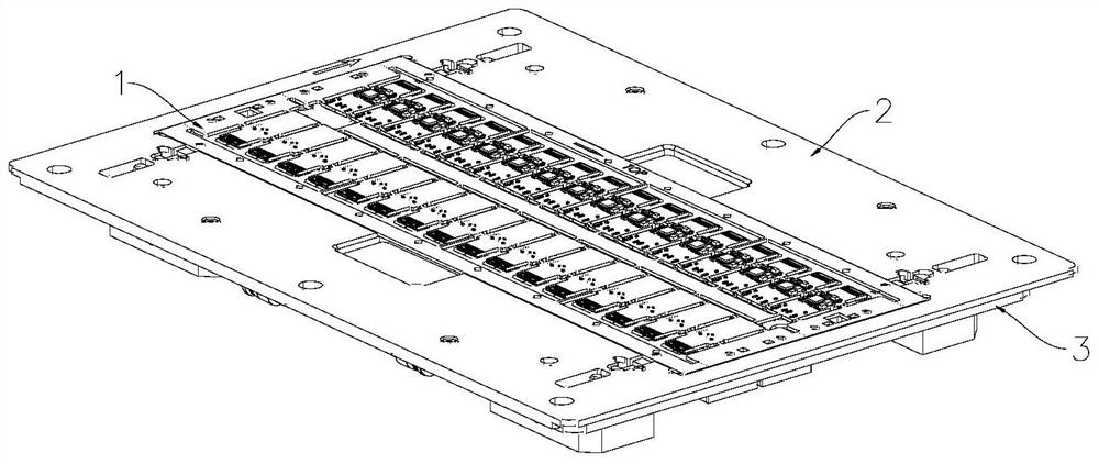
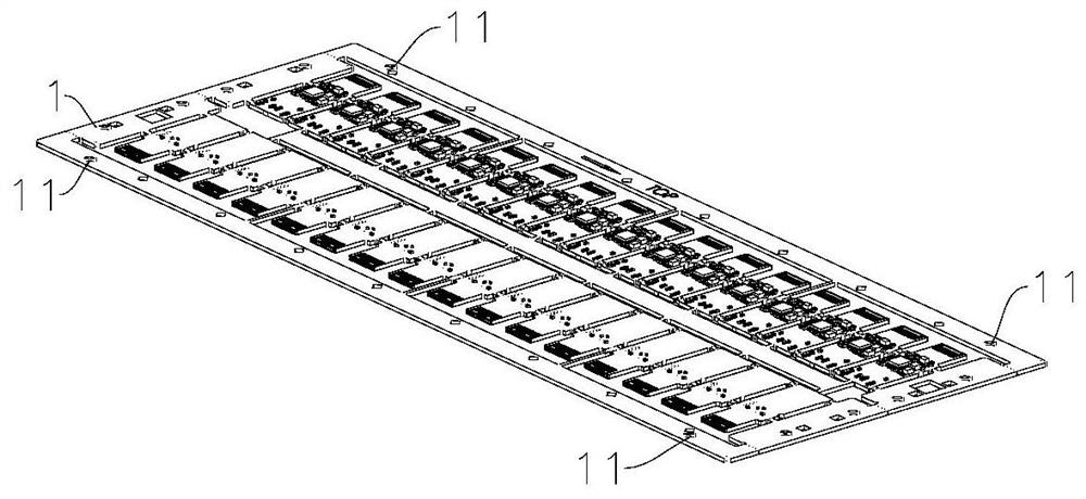
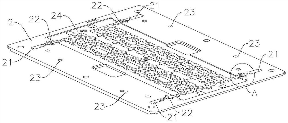
[0029] figure 1 , Figure 9 and Figure 10 A PCB unlocking jig shown includes a jig unlocking device 3 and a spring patch jig 2 arranged on the top of the jig unlocking device 3; image 3 As shown, the top surface of the spring patch fixture 2 is provided with a cavity 24 for placing the PCB board 1, the cavity 24 has a rectangular structure, and the top surface of the spring patch fixture 2 is located on two sides of the cavity 24. The outer part of the long side is provided with four elongated upper stroke holes 21 connected up and down, and the four upper stroke holes 21 correspond to the four corners of the cavity 24 respectively; Figure 5 shown and Figure 6 As shown, the position corresponding to the upper stroke hole 21 on the fixture unlocking device 3 is provided with a long strip-shaped lower stroke hole 31 connected up and down, and an u...


PUM


Abstract

The invention discloses a PCB unlocking jig which comprises a jig unlocking device and a spring patch jig arranged on the top of the jig unlocking device, a cavity used for containing a PCB is formed in the top face of the spring patch jig, an upper stroke hole is formed in the position, located on the outer side of the cavity, of the spring patch jig, and a lower stroke hole is formed in the position, corresponding to the upper stroke hole, of the jig unlocking device. Unlocking pins are arranged in the upper stroke hole and the lower stroke hole which correspond to each other up and down, and the bottoms of the unlocking pins are connected with a driving device arranged on the bottom face of the jig unlocking device. Push block grooves which are communicated with each other are formed between the upper stroke hole and the cavity, a spring push block is arranged in each push block groove, a lock pin is arranged at the top of each spring push block, and a fixing hole which can be matched with the lock pin in a sleeving manner is formed in the PCB. According to the PCB unlocking jig, the PCB can be automatically locked and unlocked, rapid transfer of the PCB between different machine types can be achieved, surface mounting and on-line testing of products are facilitated, the products are protected against bumping damage, and the product quality is guaranteed.

Description

technical field [0001] The invention relates to the field of PCB boards in the SMT industry, in particular to a PCB unlocking jig. Background technique [0002] SMT is Surface Mount Technology (Surface Mount Technology), which is the most popular technology and process in the electronic assembly industry. It is a kind of non-lead or short-lead surface mount components (referred to as SMC / SMD, Chinese called chip components) mounted on the surface of the printed circuit board (PCB) or the surface of other substrates, through reflow soldering or dipping The circuit assembly and connection technology of welding and assembly by welding and other methods. [0003] The PCB, or printed circuit board, is the carrier of the electrical connection of electronic components and one of the important components of the electronics industry. The design and manufacturing quality of the printed circuit board directly affect the quality and cost of the entire product. [0004] PCB boards need...

Claims


Application Information

Patent Timeline
Patent Type & Authority Applications(China)
IPC IPC(8): H05K3/34
CPCH05K3/341
Inventor 徐文飞刘红燕
Owner 苏州润弘安创自动化科技有限公司
Why Eureka
Try Eureka