
Semiconductor device

A semiconductor and metal plate technology, applied in the direction of semiconductor devices, semiconductor/solid-state device components, electric solid-state devices, etc., can solve the problems of setting fixed points for semiconductor modules, increasing electromagnetic noise, and controlling substrate malfunctions, etc.

Pending Publication Date: 2021-07-30
MITSUBISHI ELECTRIC CORP
View PDF12 Cites 0 Cited by
  • Summary
  • Abstract
  • Description
  • Claims
  • Application Information

AI Technical Summary

Problems solved by technology

However, regarding the range opposite to the semiconductor module, due to the limitation of the manufacturing process of the semiconductor module, it is difficult to provide a fixing point on the semiconductor module itself, so it is necessary to use other members to fix the substrate
[0005] In addition, although higher output of electric vehicles has been sought in recent years, it is known that if the output of semiconductor devices is increased, the electromagnetic noise generated by the semiconductor modules will increase, which will cause adverse effects such as malfunctions on the control board.

Method used


Image

  • Semiconductor device
  • Semiconductor device
  • Semiconductor device

Examples


Embodiment approach 1

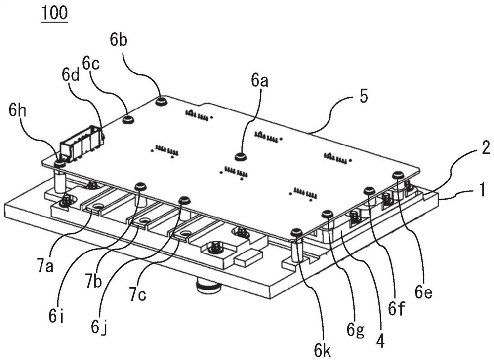
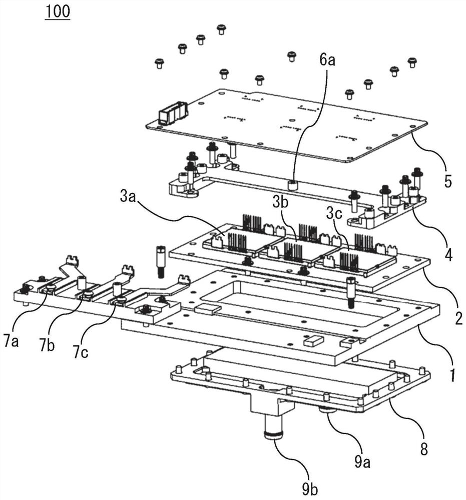
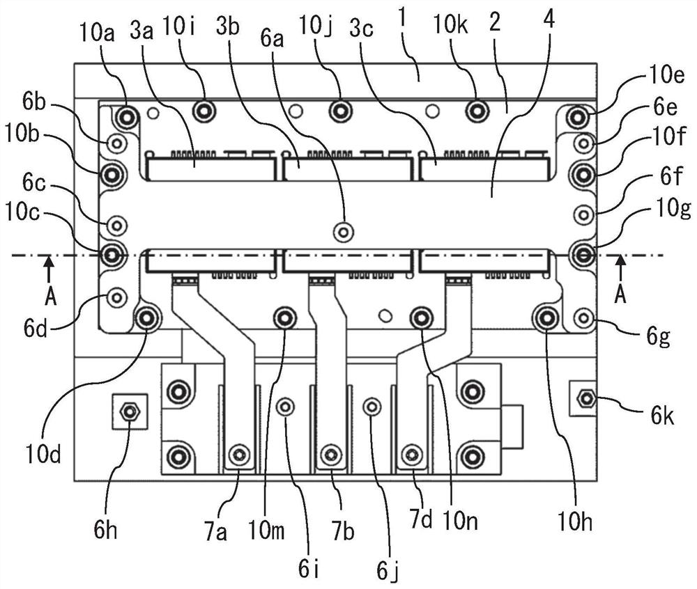
[0031] Use below Figure 1 to Figure 4 Embodiment 1 of the present application will be described. figure 1 The appearance of the semiconductor device 100 according to Embodiment 1 is shown. in addition, figure 2 A perspective view showing the overall structure of the device expanded into various structural elements is shown. exist figure 1 and figure 2 Among them, semiconductor modules 3 a , 3 b , and 3 c (hereinafter, when there are a plurality of modules, they will be described as 3 a to 3 c ) that perform power conversion are arranged on the support member 1 via the cooling plate 2 . The semiconductor modules 3a to 3c are covered by a metal plate 4 on which a control substrate 5 for controlling power conversion of the semiconductor modules 3a to 3c is provided. The control board 5 is fixed by the control board fixing parts 6 a to 6 g provided on the metal plate 4 . The control substrate fixing portion 6 a is provided to face the arrangement surface of the semiconduc...

Embodiment approach 2

[0052] Below, based on Figure 9 , Embodiment 2 of the present application will be described. Figure 9 With Figure 6 Cutaway view of the same main parts. Such as Figure 9 As shown, the semiconductor device of this embodiment includes a support member 1, a cooling plate 2, semiconductor modules 3a to 3c mounted on the cooling plate 2 and performing power conversion, a first metal plate 4b disposed on the cooling plate 2, and mounted on the cooling plate 2. The first control substrate 5a on the first metal plate 4b, the second metal plate 4c mounted on the first metal plate 4b, the second control substrate 5b arranged on the second metal plate 4c, and the bottom plate 8 constituting the cooling water flow path . Although omitted in this figure, normally, the first control board 5 a and the second control board 5 b are connected using an FPC, a wire harness, or an inter-board connector.

[0053] The signal terminal pins 11a-11f of the semiconductor modules 3a-3c are conne...


PUM


Abstract

A semiconductor device is provided with: semiconductor modules (3a, 3b, 3c) disposed on a support member (1) via a cooling plate (2); and a metal plate (4) for supporting a control substrate (5) for controlling the semiconductor module, the metal plate being supported by the support member, covering the semiconductor module, and fixing the control substrate so as to face the installation surface of the semiconductor module.

Description

technical field [0001] The present invention relates to semiconductor devices. Background technique [0002] In an electric vehicle or a hybrid vehicle driven by an electric motor, a semiconductor device mounted with a semiconductor module such as a power module is used. Semiconductor devices mounted on vehicles require space efficiency in the vehicle, and the number of mounted devices increases due to electrification, and the layout space decreases. Therefore, the semiconductor device itself needs to be miniaturized and mounted directly on the motor or transmission. Since a motor or a transmission generates strong vibrations when driven, semiconductor devices require extremely high vibration resistance. [0003] A semiconductor module of such a semiconductor device mounted on a vehicle includes a connection terminal connected to a wiring electrode and a connection terminal to a control board. Usually, the signal terminals of the semiconductor module and the control substr...

Claims


Application Information

Patent Timeline
Patent Type & Authority Applications(China)
IPC IPC(8): H05K7/14H05K9/00
CPCH05K7/1432H05K9/002H05K9/0026H01L23/473H01L23/4006H01L23/552H01L25/072H01L25/18H01L25/0655H01L2023/4087H01L23/49H01L23/367
Inventor 冈宽晴
Owner MITSUBISHI ELECTRIC CORP
Learn More