
Optical thin film with double-sided structure and manufacturing method thereof

A technology of optical film and double-sided structure, which is applied in the direction of optics, optical elements, and photoplate-making process of pattern surface, etc. It can solve the problems of increasing the thickness of optical film and reducing the light transmittance of optical film, so as to achieve the effect of reducing thickness

Inactive Publication Date: 2021-08-03
SHINE OPTOELECTRONICS KUNSHAN CO LTD
View PDF7 Cites 1 Cited by
  • Summary
  • Abstract
  • Description
  • Claims
  • Application Information

AI Technical Summary

Problems solved by technology

[0007] Although optical films have had a revolutionary impact on our lives, since each optical film retains a substrate inside, the substrate increases the thickness of the optical film, thereby reducing the light transmittance of the optical film

Method used


Image

  • Optical thin film with double-sided structure and manufacturing method thereof
  • Optical thin film with double-sided structure and manufacturing method thereof
  • Optical thin film with double-sided structure and manufacturing method thereof

Examples


Embodiment Construction

[0044] In order to enable those skilled in the art to better understand the technical solutions in the present application, the technical solutions in the embodiments of the present application will be clearly and completely described below in conjunction with the drawings in the embodiments of the present application. Obviously, the described The embodiments are only some of the embodiments of the present application, but not all of them. Based on the embodiments in this application, all other embodiments obtained by persons of ordinary skill in the art without making creative efforts shall fall within the protection scope of the present invention.

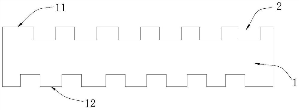
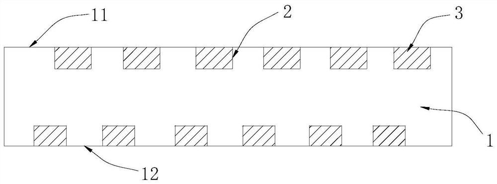
[0045] It should be noted that when an element is referred to as being “disposed on” another element, it may be directly on the other element or there may also be an intervening element. When an element is referred to as being "connected to" another element, it can be directly connected to the other element or intervening element...


PUM

PropertyMeasurementUnit
visible light transmittanceaaaaaaaaaa
reflectivityaaaaaaaaaa

Abstract

The invention discloses an optical thin film with a double-sided structure and a manufacturing method thereof. The optical thin film with the double-sided structure comprises a polymer body provided with a first surface and a second surface which are opposite to each other, and an accommodating mechanism which is arranged on the first surface and the second surface and is used for forming an image-text structure on the surface of the body, wherein the body with the accommodating mechanism is of an integrated structure; the accommodating mechanism comprises a groove; a filler is accommodated in the accommodating mechanism to form the image-text structure; the filler comprises one or more of a conductive material, a coloring material and a dyeing material; the polymer comprises thermocuring resin and / or photocuring resin; and the light transmittance of the body is 0.7 or above. The optical thin film with the double-sided structure and the manufacturing method thereof provided by the invention are beneficial to reducing the thickness of the optical thin film.

Description

[0001] This application is a divisional application of the case of application number 201510397170.2, application date July 8, 2015, and invention name "double-sided structured optical film and its manufacturing method". technical field [0002] The present application relates to the technical field of optical thin films, in particular to an optical thin film with a double-sided structure and a manufacturing method thereof. Background technique [0003] Optical film is a modern product integrating imprinting technology, micro-nano processing technology, and imaging technology. It has broad market prospects in touch screens, anti-counterfeiting labels, packaging and other fields. [0004] In the field of touch screens, optical thin films can be used to make transparent conductive films, such as the invention patent "Double-sided patterned transparent conductive film and its preparation method" with application number 201210141850.4. This patent uses embossing technology to ma...

Claims


Application Information

Patent Timeline
Patent Type & Authority Applications(China)
IPC IPC(8): G02B1/10G02B1/04G03F7/00
Inventor 张健
Owner SHINE OPTOELECTRONICS KUNSHAN CO LTD
Features
  • Generate Ideas
  • Intellectual Property
  • Life Sciences
  • Materials
  • Tech Scout
  • Unparalleled Data Quality
  • Higher Quality Content
  • 60% Fewer Hallucinations
Learn More