PCB jointed board determination method and device, electronic equipment and storage medium

A panel and single panel technology, applied in the field of electronics, can solve the problems of high design cost, inability to balance panel quality and utilization rate, etc., and achieve the effect of reducing utilization rate, reducing warpage risk, and reducing loss

Pending Publication Date: 2021-08-03
QUECTEL WIRELESS SOLUTIONS
View PDF6 Cites 1 Cited by
  • Summary
  • Abstract
  • Description
  • Claims
  • Application Information

AI Technical Summary

Problems solved by technology

[0003] In view of this, the purpose of this application is to provide a PCB panel determination method, device, electronic equipment and storage medium, so as to improve the problems of high design cost and inability to take into account the quality and utilization rate of the existing panel design.

Method used


Image

  • PCB jointed board determination method and device, electronic equipment and storage medium
  • PCB jointed board determination method and device, electronic equipment and storage medium
  • PCB jointed board determination method and device, electronic equipment and storage medium

Examples


Embodiment approach

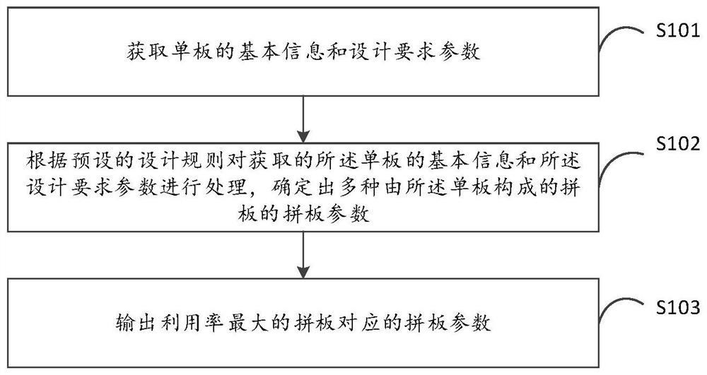
[0041] In one embodiment, the processing procedure of step S102 may be as follows figure 2 shown. Including the following steps:

[0042] Step S201: Determine the maximum size allowed by the panel according to the preset design rules and the minimum pad step.

[0043] For example, the preset design rules stipulate that: the minimum pad step ≤ 0.20mm, the maximum size allowed for the panel is 100*100mm; 0.2mm 0.35mm, the maximum size allowed for the panel is 200*200mm. Assuming that the minimum pad step is 0.35mm, according to the preset design rules and the minimum pad step, it can be determined that the maximum size allowed by the panel is 150*150mm.

[0044] Step S202: According to the preset design rules, the length of the veneer, and the thickness of the veneer, determine the maximum panelization mode allowed for panelization.

[0045] For example, the preset design rule stipulates that if the plate thickness is 35*35mm, the maximum allowable combination method is 3 p...


PUM


Abstract

The invention relates to a PCB jointed board determination method and device, electronic equipment and a storage medium, and belongs to the technical field of electronics. The method is applied to the electronic equipment and comprises the following steps: acquiring basic information and design requirement parameters of a single board; according to a preset design rule, processing the obtained basic information of the single boards and the design requirement parameters, and determining multiple jointed board parameters of jointed boards formed by the single boards, wherein the preset design rule is obtained by processing the jointed board parameters of multiple PCB jointed boards meeting the industrial standard; and outputting the jointed board parameter corresponding to the jointed board with the maximum utilization rate. According to the method, the design rule considering the quality and the utilization rate of the jointed board is obtained by processing the jointed board parameters of the plurality of PCB jointed boards meeting the industrial standard, so the optimal jointed board scheme can be quickly obtained only by inputting the basic information and the design requirement parameters of the single board during the subsequent jointed board design.

Description

technical field [0001] The present application belongs to the field of electronic technology, and in particular relates to a PCB panel determination method, device, electronic equipment and storage medium. Background technique [0002] In order to meet the production needs in the electronics industry, it is necessary to combine the used PCB (Printed Circuit Board, printed circuit board) veneers into a jigsaw board (a large board formed by combining multiple veneers according to certain rules). The different designs of the jigsaw boards will affect the warping of the veneers, the placement accuracy, the utilization rate, the speed of the board splitting (the boards are cut and divided by CNC (Computerized Numerical Control, computer numerical control technology) etc.) speed, The wear and tear of the parts of the splitter, etc. The current panel design makes it impossible to achieve a balance between the quality of the panel and the utilization rate. It is often designed thro...

Claims


Application Information

Patent Timeline
Patent Type & Authority Applications(China)
IPC IPC(8): G06F30/392G06F30/398G06F115/12
CPCG06F30/392G06F30/398G06F2115/12
Inventor 刘新亮郑雷
Owner QUECTEL WIRELESS SOLUTIONS
Why Eureka
Try Eureka