Latch structure and latch method
A buffer register and flip-flop technology, applied in the field of latching, can solve the problems of occupying a large chip area, high power consumption, signal loss, etc., achieving the effect of small area overhead, low power consumption, and preventing information loss
- Summary
- Abstract
- Description
- Claims
- Application Information
AI Technical Summary
Problems solved by technology
Method used
Image


Examples
Embodiment 1
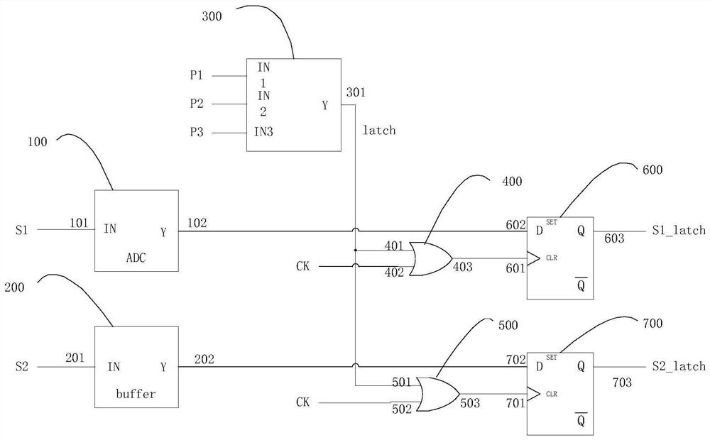
[0052] Such as figure 1 As shown: a latch structure is disclosed, which realizes zero power consumption latch, occupies a very small chip area, increases the probability of latch failure after power failure, realizes encrypted latch and reset, and realizes power loss electrical latch.
[0053] It includes an analog-to-digital conversion circuit 100, including an analog signal receiving end 101 and a first digital signal output end 102;
[0054] The buffer register 200 includes a digital signal receiving end 201 and a second digital signal output end 202;
[0055] Encryption circuit 300, including at least one set of frequency circuits, control signal input terminals corresponding to the number of frequency division circuits, and an encrypted signal output terminal 301;
[0056] The first OR gate 400 includes a first clock signal input terminal 401, a first encrypted signal input terminal 402 and a first OR gate output terminal 403;
[0057] The second OR gate 500 includes a...
Embodiment 2
[0091] This embodiment discloses a latching method based on the latching circuit in Embodiment 1, and specifically relates to a method for realizing zero-power latching, occupying a very small chip area, and increasing the latching capacity of the latch after power-off. Probability of failure, realize encrypted latch and reset, realize power-down latch:
[0092] (1) Latching of analog signals
[0093] converting the analog signal into a first digital signal, and inputting the first digital signal to a first data input terminal of a first flip-flop;
[0094] Separately divide and process at least one group of control signals, and output encrypted signals after the frequency-divided control signals pass through AND gate logic;
[0095] inputting the encrypted signal as a clock signal of the first flip-flop to a clock terminal of the first flip-flop, and outputting latched data;
[0096] Specifically, the input analog signal S1 is converted by the analog-to-digital conversion c...
Embodiment 3
[0113] In this embodiment, the difference from Embodiment 1 is that the encryption circuit uses a frequency division circuit, such as a frequency division circuit of 8 or a frequency division circuit of 10, and removes the three-input AND gate in Embodiment 1, and finally The Q terminal of the first-level D flip-flop outputs to the OR gate.
[0114] It should also be noted that in the structural naming of this technical solution, there is no functional specificity, such as "encryption circuit" and "encryption signal", which do not refer to the meaning of only encryption function, and the actual technology of "encryption circuit" The meanings of the descriptions of the features are based on the examples of this embodiment.
PUM
 Abstract
Description
Claims
Application Information