Method for manufacturing light-emitting device using laser etching and manufacturing device thereof

A light-emitting device, laser etching technology, applied in the manufacture of semiconductor/solid-state devices, electric solid-state devices, semiconductor devices, etc., can solve the problems of mask/nozzle/pen tip clogging, wall formation, and spotting, etc., to reduce the light-emitting device. The effect of reducing defects and increasing process time

Pending Publication Date: 2021-08-06
KYONGGI UNIV IND & ACAD COOPERATION FOUND
View PDF0 Cites 0 Cited by
  • Summary
  • Abstract
  • Description
  • Claims
  • Application Information

AI Technical Summary

Problems solved by technology

However, these physical patterning methods will cause clogging of masks / nozzles / tips, generation of spots, formation of walls, pattern reduction, etc., which will lead to increased process defect rates
Moreover, since the finer and finer the pattern of the light-emitting layer, this phenomenon will occur more frequently, which has become a great obstacle to ultra-high-resolution fine patterning technology.
In addition, the chemical patterning method uses the chemical reaction of quantum dots, and the difference in chemical resistance of quantum dots will be utilized.
However, although the above-mentioned chemical patterning method can ensure the uniformity of patterned ultra-fine quantum dot devices, there is a problem that the quantum dot luminescence characteristics are reduced, and the quantum dot materials that can be used are very limited.

Method used


Image

  • Method for manufacturing light-emitting device using laser etching and manufacturing device thereof
  • Method for manufacturing light-emitting device using laser etching and manufacturing device thereof
  • Method for manufacturing light-emitting device using laser etching and manufacturing device thereof

Examples


Embodiment Construction

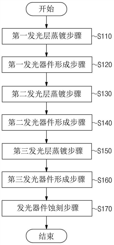
[0042] Hereinafter, a method for manufacturing a light-emitting device using laser etching and a manufacturing device therefor according to an embodiment of the present invention will be described with reference to the accompanying drawings.

[0043] First, a method of manufacturing a light emitting device by laser etching according to an embodiment of the present invention will be described.

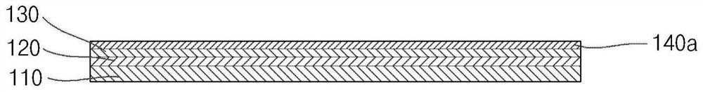
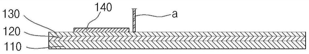
[0044] figure 1 It is a flow chart of a method for manufacturing a light emitting device using laser etching according to an embodiment of the present invention. figure 2 It is a process diagram of the evaporation step of the first light-emitting layer in the manufacturing method of the light-emitting device by laser etching according to an embodiment of the present invention. image 3 It is a process diagram of the first light emitting device forming step in the light emitting device manufacturing method using laser etching according to an embodiment of the present invention. Figur...


PUM

PropertyMeasurementUnit
thicknessaaaaaaaaaa
thicknessaaaaaaaaaa

Abstract

The present disclosure discloses a method for manufacturing a light-emitting device using laser etching and a manufacturing device thereof. The method for manufacturing a light-emitting device using laser etching includes: a first light-emitting layer forming step for depositing a first light-emitting layer on an surface of a hole transport layer deposited on an upper surface of an anode substrate; a first light-emitting device forming step for etching the first light-emitting layer to form a first light-emitting device; a second light-emitting layer depositing step for depositing a second light-emitting layer on a region including the upper surface of the hole transport layer; a second light-emitting device forming step for etching the second light-emitting layer to form a second light-emitting device; a third light-emitting layer depositing step for depositing a third light-emitting layer on a region including the upper surface of the hole transport layer; and a third light-emitting device forming step for etching the third light-emitting layer to form a third light-emitting device.

Description

technical field [0001] The present invention relates to a method of manufacturing a light emitting device constituting a flat panel display panel and an apparatus therefor. Background technique [0002] Light-emitting devices used in flat panel display panels include organic light-emitting diodes (Organic Light-Emitting Diode; OLED) and quantum dot light-emitting diodes (Quantum dot light-emitting diodes; QLED). [0003] Organic light-emitting diodes stack anode (Anode) electrodes, hole injection layers (HIL), hole transport layers (HTL), light emitting layers (EML), electron transport layers (ETL), electron injection layers (EIL) and cathode electrodes in sequence. (Cathode) made. And, the above-mentioned organic light emitting diode may exhibit colors by forming a light emitting layer into a red (R) light emitting device, a green (G) light emitting device, and a blue (B) light emitting device. [0004] The above-mentioned red (R) light-emitting device, green (G) light-em...

Claims


Application Information

Patent Timeline
Patent Type & Authority Applications(China)
IPC IPC(8): H01L51/56H01L51/00
CPCH10K71/231H10K71/00H10K59/35H10K50/115H10K50/11H10K2102/351
Inventor 朱祥玄
Owner KYONGGI UNIV IND & ACAD COOPERATION FOUND
Why Eureka
Try Eureka