Light-emitting diode chip and manufacturing method thereof

A technology of light-emitting diodes and chips, which is applied in the direction of electrical components, circuits, semiconductor devices, etc., can solve problems such as information leakage, and achieve the effects of reducing possibility, good display directionality, and avoiding display information leakage

Active Publication Date: 2021-08-20
HC SEMITEK ZHEJIANG CO LTD
View PDF10 Cites 0 Cited by
  • Summary
  • Abstract
  • Description
  • Claims
  • Application Information

AI Technical Summary

Problems solved by technology

However, if there is no difference in the display screen, the people around the user can also clearly see the information on the user's screen, resulting in the risk of information leakage

Method used


Image

  • Light-emitting diode chip and manufacturing method thereof
  • Light-emitting diode chip and manufacturing method thereof
  • Light-emitting diode chip and manufacturing method thereof

Examples


Embodiment Construction

[0040] In order to make the purpose, technical solution and advantages of the present disclosure clearer, the implementation manners of the present disclosure will be further described in detail below in conjunction with the accompanying drawings.

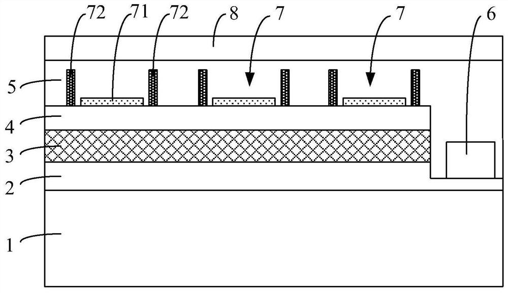
[0041] figure 1 is a schematic structural diagram of a light-emitting diode chip provided by an embodiment of the present disclosure, as shown in figure 1 As shown, the LED chip includes a substrate 1 , an N-type semiconductor layer 2 , an active layer 3 , a P-type semiconductor layer 4 , an insulating layer 5 and an N-type electrode 6 . The N-type semiconductor layer 2 , the active layer 3 and the P-type semiconductor layer 4 are sequentially stacked on the surface of the substrate 1 . The P-type semiconductor layer 4 is provided with a groove extending to the N-type semiconductor layer 2, and the N-type electrode 6 is arranged on the N-type semiconductor layer 2 in the groove.

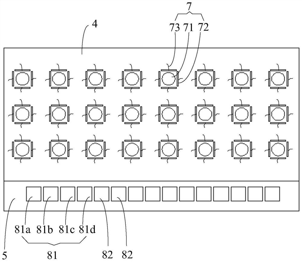
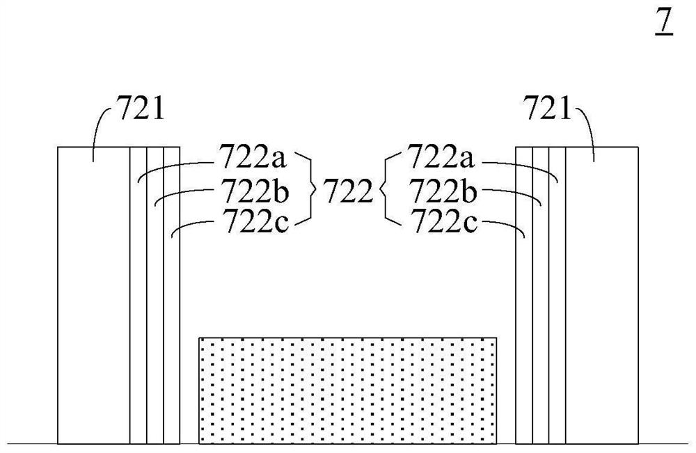
[0042] The LED chip also includes a plurality of ...


PUM

PropertyMeasurementUnit
thicknessaaaaaaaaaa
thicknessaaaaaaaaaa
thicknessaaaaaaaaaa

Abstract

The invention provides a light-emitting diode chip and a manufacturing method thereof, and belongs to the technical field of semiconductors. The light-emitting diode chip further comprises a plurality of light-emitting adjusting assemblies located on a P-type semiconductor layer, the light-emitting adjusting assemblies are arranged on the P-type semiconductor layer in an array mode, the structures of the light-emitting adjusting assemblies are the same, each light-emitting adjusting assembly comprises an indium tin oxide unit, a plurality of light-transmitting walls and a plurality of first control wires, the plurality of light-transmitting walls are arranged at intervals in the circumferential direction of the indium tin oxide unit, one end of each first control wire is connected with one light-transmitting wall, the first control wires are used for receiving first control signals and transmitting the first control signals to the light-transmitting walls, and the first control signals are used for changing the size of an electric field in the light-transmitting walls so as to adjust the light transmission of the light-transmitting walls. The LED chip can control the light emitting direction of the side surface of the light-emitting diode chip, so that the display screen reaches a display angle expected by a user, the use experience of the user is improved, and the leakage of display information is avoided.

Description

technical field [0001] The present disclosure relates to the technical field of semiconductors, in particular to a light emitting diode chip and a manufacturing method thereof. Background technique [0002] A light emitting diode (English: Light Emitting Diode, referred to as: LED) is a semiconductor device that can emit light. By using different semiconductor materials and structures, LEDs can cover a full color range from ultraviolet to infrared, and have been widely used in economic life such as display, decoration, and communication. [0003] At present, the display screens of personal electronic products such as mobile phones are gradually adopting LED display planes. The current LED chips all emit light directly to form a display screen, and the viewing angle of the light can reach about 160 degrees, and there is no difference in each direction. However, if there is no difference in the display screen, people around the user can also clearly see the information on th...

Claims


Application Information

Patent Timeline
Patent Type & Authority Applications(China)
IPC IPC(8): H01L33/58H01L33/62H01L33/00
CPCH01L33/58H01L33/62H01L33/0075H01L33/0066H01L2933/0058H01L2933/0066
Inventor 兰叶王江波吴志浩
Owner HC SEMITEK ZHEJIANG CO LTD
Why Eureka
Try Eureka