Pixel processing circuit, method and device and electronic equipment

A technology for processing circuits and pixels, applied in the field of communications, can solve problems such as poor image quality, and achieve the effects of reducing noise components, improving image quality, and suppressing image noise.

Active Publication Date: 2021-08-20
VIVO MOBILE COMM HANGZHOU CO LTD
View PDF11 Cites 3 Cited by
  • Summary
  • Abstract
  • Description
  • Claims
  • Application Information

AI Technical Summary

Problems solved by technology

[0004] The purpose of the embodiments of the present application is to provide a pixel processing circuit, method, device, and electronic equipment, which can solve the problem of poor image quality of images captured by electronic equipment

Method used


Image

  • Pixel processing circuit, method and device and electronic equipment
  • Pixel processing circuit, method and device and electronic equipment
  • Pixel processing circuit, method and device and electronic equipment

Examples


Embodiment 1

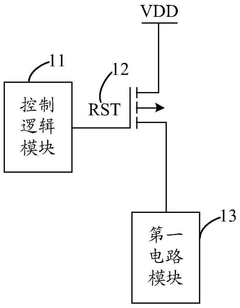
[0036] An embodiment of the present application provides a pixel processing circuit, figure 1 A pixel processing circuit provided by the embodiment of the present application is shown. Such as figure 1As shown, the pixel processing circuit may include: a control logic module 11 , a first reset transistor (Reset, RST) reset gate 12 and a first circuit module 13 .

[0037] Wherein, one end of the control logic module 11 (also called a control logic device) is connected to one end of the first RST reset gate 12 , and the other end of the first RST reset gate 12 is connected to the first circuit module 13 . The control logic module 11 is used to control the first RST reset gate 12 to be in the first working state when receiving the first control signal; the first RST reset gate 12 is used to adjust the Corresponding to the exposure of the pixels of the three channels; the first circuit module 13 is used to process the light corresponding to the shooting object.

[0038] It shou...

Embodiment 2

[0080] It should be noted that the pixel processing method in the embodiment of the present application can be applied to electronic equipment, a pixel processing device, or a lens module.

[0081] An embodiment of the present application provides a pixel processing method, Figure 8 shows a flow chart of a pixel processing method provided by an embodiment of the present application, as shown in Figure 8 As shown, the pixel processing method provided by the embodiment of the present application may include the following steps 201 and 202 .

[0082] Step 201, the electronic device acquires at least one trigger time of a first control signal.

[0083] In the embodiment of the present application, the above-mentioned first control signal is used to control and adjust the exposure of the pixels of the three channels corresponding to the shooting object, and each trigger time of the at least one trigger time corresponds to one of the three channels.

[0084] In the embodiment of...


PUM


Abstract

The invention discloses a pixel processing circuit, method and device and electronic equipment, belongs to the technical field of communication, and can solve the problem that the image quality of an image shot by the electronic equipment is poor. The pixel processing circuit comprises a control logic module, a first RST reset gate and a first circuit module. One end of the control logic module is connected with one end of the first RST reset gate, and the other end of the first RST reset gate is connected with the first circuit module; the control logic module is used for controlling the first RST reset gate to be in a first working state under the condition that a first control signal is received, the first RST reset gate is used for adjusting the exposure of pixels of three channels corresponding to a shooting object in the first working state, and the first circuit module is used for processing light corresponding to the shooting object. The three-channel pixel processing method and device are applied to the three-channel pixel processing process.

Description

technical field [0001] The present application belongs to the technical field of communication, and in particular relates to a pixel processing circuit, method, device and electronic equipment. Background technique [0002] Generally, in order to improve the image quality of the image captured by the electronic device, it can be achieved by increasing the signal-to-noise ratio of the image. Specifically, after the external light (that is, the light corresponding to the object to be photographed) passes through the lens of the electronic device, when filtered by an infrared filter, the light transmittance of the light can be increased to increase the light transmitted to the sensor (sensor). The signal intensity value of the light on the photosensitive diode (pixel), so as to achieve the purpose of improving the signal-to-noise ratio of the image; and the photosensitive diode can convert the perceived light signal into an electrical signal, through the amplification circuit a...

Claims


Application Information

Patent Timeline
Patent Type & Authority Applications(China)
IPC IPC(8): H04N5/235H04N5/353H04N5/378H04N5/3745H04N5/374H04N5/369H04N5/357H04N5/363H04N5/217H04N5/225
CPCH04N25/60H04N23/50H04N23/54H04N23/57H04N23/55H04N23/73H04N25/53H04N25/616H04N25/65H04N25/70H04N25/76H04N25/77H04N25/75
Inventor 李沛德龚柳青
Owner VIVO MOBILE COMM HANGZHOU CO LTD
Why Eureka
Try Eureka