Supercharge Your Innovation With Domain-Expert AI Agents!

Wafer bonding method and wafer bonding equipment

A wafer bonding and wafer technology, applied in the direction of electrical components, semiconductor/solid-state device manufacturing, circuits, etc., can solve problems affecting bonding waves, edge distortion, affecting life, etc., to reduce the impact of wafer deformation , reducing the effect of distortion

Pending Publication Date: 2021-08-24
WUHAN XINXIN SEMICON MFG CO LTD
View PDF0 Cites 2 Cited by
  • Summary
  • Abstract
  • Description
  • Claims
  • Application Information

AI Technical Summary

Problems solved by technology

In addition, the drastic change of force will cause the wear of the vacuum belt and affect the service life
[0008] (4) The upper wafer 03 falls by gravity, and the falling process is uncontrolled. The bonding wave expands from the center to the surroundings to complete the wafer bonding. The falling of the edge area will affect the expansion of the bonding wave to the surroundings, resulting in large edge distortion

Method used


Image

  • Wafer bonding method and wafer bonding equipment
  • Wafer bonding method and wafer bonding equipment
  • Wafer bonding method and wafer bonding equipment

Examples


Embodiment Construction

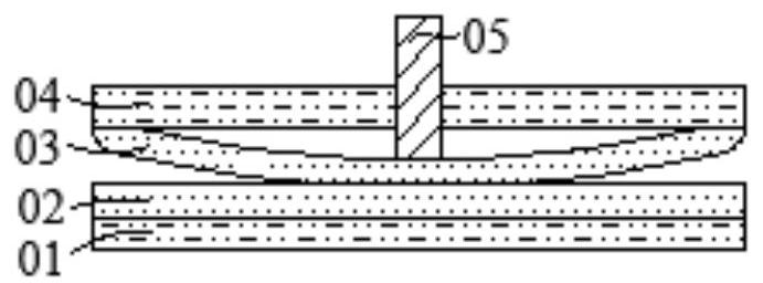
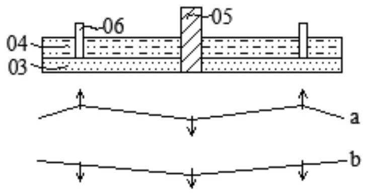
[0038] Embodiments of the present invention provide a wafer bonding method and wafer bonding equipment. The present invention will be described in further detail below in conjunction with the accompanying drawings and specific embodiments. The advantages and features of the present invention will become clearer from the following description. It should be noted that the drawings are all in a very simplified form and use imprecise scales, and are only used to facilitate and clearly assist the purpose of illustrating the embodiments of the present invention.

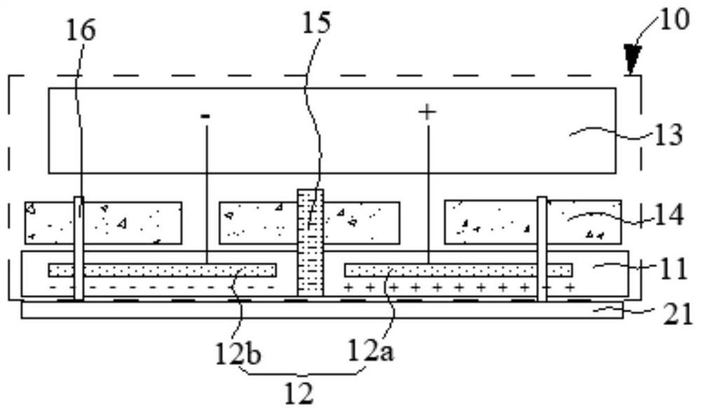
[0039] An embodiment of the present invention provides a wafer bonding equipment, including:

[0040] An electrostatic adsorption chuck, the electrostatic adsorption chuck provides adjustable electrostatic adsorption force for the wafer to be bonded;

[0041] The electrostatic adsorption chuck includes a dielectric layer and an electrode layer embedded in the dielectric layer, the electrode layer includes a positive elec...


PUM


Abstract

The invention provides a wafer bonding method and wafer bonding equipment, and the method comprises the steps: enabling an electrostatic adsorption chuck to adsorb an upper wafer through electrostatic adsorption force, enabling a lower wafer to be fixed on a lower chuck, and enabling the upper wafer to be aligned with the lower wafer; pressing an ejector pin of the electrostatic adsorption chuck down the central area of the upper wafer, so that the upper wafer bends downwards and is in contact with the central area of the lower wafer; and adjusting the size of the electrostatic adsorption force, so that the upper wafer is gradually separated from the electrostatic adsorption chuck under the action of the gravity and the electrostatic adsorption force and is bonded with the lower wafer. An upper wafer is adsorbed through an electrostatic adsorption chuck, and in the process that the upper wafer falls and is bonded with a lower wafer, the upper wafer is gradually separated from the electrostatic adsorption chuck under the action of the gravity and the electrostatic adsorption force by adjusting the size of the electrostatic adsorption force, so that the process is controllable in the falling process of the upper wafer, the extension of bonding waves from the center to the periphery is not influenced, and wafer bonding is completed; and meanwhile, distortion of the wafer caused by a vacuum chuck vacuum adsorption mode is reduced.

Description

technical field [0001] The invention belongs to the technical field of integrated circuit manufacturing, and in particular relates to a wafer bonding method and wafer bonding equipment. Background technique [0002] With the continuous development of semiconductor technology, wafer bonding technology has been widely used. Bonding two or more wafers can effectively increase the number of devices per unit area. [0003] Such as figure 1 and figure 2 As shown, in the conventional bonding process, the upper chuck 04 is a vacuum chuck that absorbs the upper wafer 03 by vacuum, and the lower wafer 02 is fixed on the lower chuck 01 . After the upper wafer 03 and the lower wafer 02 are aligned, the thimble (Piston) 05 located in the central area of ​​the upper chuck 04 presses down on the upper wafer 03, causing the upper wafer 03 to bend downward and then move After reaching a certain distance, the central vacuum belt of the upper wafer 03 starts to release the vacuum, and the ...

Claims


Application Information

Patent Timeline
Patent Type & Authority Applications(China)
IPC IPC(8): H01L21/18H01L21/67H01L21/683H01L21/68
CPCH01L21/187H01L21/67011H01L21/6831H01L21/68
Inventor 吴星鑫
Owner WUHAN XINXIN SEMICON MFG CO LTD
Features
  • R&D
  • Intellectual Property
  • Life Sciences
  • Materials
  • Tech Scout
  • Unparalleled Data Quality
  • Higher Quality Content
  • 60% Fewer Hallucinations
Learn More