Three-dimensional integrated high-efficiency heat dissipation packaging structure and preparation method thereof

A packaging structure and high-efficiency technology, which is applied in the manufacture of semiconductor/solid-state devices, electric solid-state devices, semiconductor devices, etc., can solve problems such as high cost, high technical difficulty, and failure to consider the air cavity of microwave power chips, so as to meet electromagnetic compatibility The effect of sexual demands

Active Publication Date: 2021-08-24
SOUTHWEST CHINA RES INST OF ELECTRONICS EQUIP
View PDF23 Cites 0 Cited by
  • Summary
  • Abstract
  • Description
  • Claims
  • Application Information

AI Technical Summary

Problems solved by technology

[0003] At present, there are many patents on three-dimensional integrated high-efficiency heat dissipation structures: for example, Chinese patent ZL201811374347.7 proposes a three-dimensional active heat dissipation packaging structure embedded in micro-channels and its manufacturing process, which realizes three-dimensional integration of efficient heat dissipation structures; however, this patent The air cavity problem of the microwave power chip is not considered
Chinese patent ZL201810601226.5 proposes a three-dimensional heterogeneous structure packaging method for heat dissipation of high-power GaN devices, which realizes three-dimensional integration for microwave applications; high cost
[0004] How to construct a three-dimensional integrated high-efficiency heat dissipation packaging structure for typical microwave multi-chip module applications, while achieving high heat flux dissipation and meeting the electromagnetic compatibility requirements of microwave signals, is still rarely reported.

Method used


Image

  • Three-dimensional integrated high-efficiency heat dissipation packaging structure and preparation method thereof
  • Three-dimensional integrated high-efficiency heat dissipation packaging structure and preparation method thereof
  • Three-dimensional integrated high-efficiency heat dissipation packaging structure and preparation method thereof

Examples


Embodiment Construction

[0037] The present invention will be further described below in conjunction with the accompanying drawings.

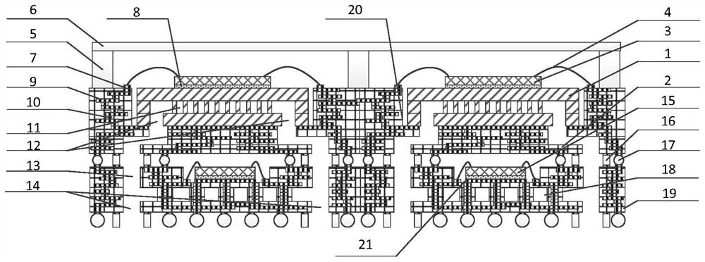
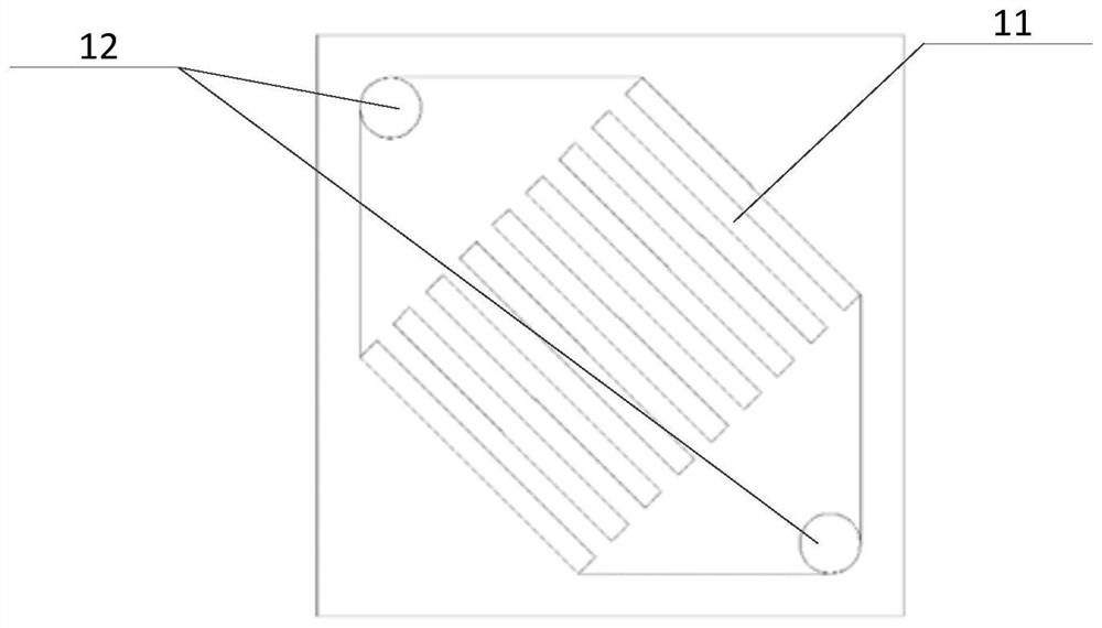
[0038] Such as Figure 1-Figure 5 As shown, a three-dimensional integrated high-efficiency heat dissipation packaging structure includes: a first packaging substrate 2, a second packaging substrate 19, a heat dissipation microchannel 1, a first chip 3, a second chip 15, a cover plate 6, a surrounding frame 5, Liquid cooling connector 16 and electrical connector 17;

[0039] The heat dissipation micro-channel 1 and the surrounding frame 5 are welded on the first packaging substrate 2;

[0040] The first chip 3 is welded on the heat dissipation micro-channel 1 and interconnected with the surface pad of the first package substrate 2; the second chip 15 is welded on the second package substrate 1 and connected with the surface pad of the second package substrate 19 interconnected;

[0041] The cover plate 6 is welded on the surrounding frame 5 for sealing;

[0042] The...


PUM


Abstract

The invention relates to the technical field of microelectronic heat dissipation, and particularly discloses a three-dimensional integrated efficient heat dissipation packaging structure and a preparation method thereof. The packaging structure comprises a first packaging substrate, a second packaging substrate, a heat dissipation micro-channel, a first chip, a second chip, a cover plate, an enclosure frame, a liquid cooling connector and an electric connector; the heat dissipation micro-channel and the enclosure frame are welded on the first packaging substrate; the first chip is welded on the heat dissipation micro-channel and is interconnected with a surface bonding pad of the first packaging substrate; the second chip is welded on the second packaging substrate and is interconnected with a surface bonding pad of the second packaging substrate; the cover plate is welded on the enclosure frame for sealing; and the liquid cooling connector and the electric connector are welded between the first packaging substrate and the second packaging substrate, and the liquid cooling connector and the electric connector are also welded on the second packaging substrate. According to the invention, the electromagnetic compatibility requirement of microwave signals can be met while high-heat-flux heat dissipation is realized.

Description

technical field [0001] The invention relates to the field of microelectronic heat dissipation technology, in particular to a three-dimensional integrated high-efficiency heat dissipation packaging structure and a preparation method thereof. Background technique [0002] With the development of microelectronics technology, the integration density of electronic systems is gradually increasing. The traditional planar high-density integration method can no longer meet the application requirements. It is necessary to use three-dimensional integration technology to change the traditional planar integration method into a three-dimensional integration method. At the same time, the widespread use of third-generation semiconductor technologies represented by GaN has gradually increased the power density of microwave power devices. Correspondingly, the heat flux density of power chips is increasing day by day, and thermal management has gradually become one of the technical bottlenecks...

Claims


Application Information

Patent Timeline
Patent Type & Authority Applications(China)
IPC IPC(8): H01L23/467H01L23/473H01L23/367H01L23/373H01L23/538H01L23/552H01L21/48H01L21/768
CPCH01L23/473H01L23/367H01L23/467H01L23/5384H01L23/5386H01L23/3731H01L21/4882H01L21/76897H01L21/76895H01L23/552
Inventor 张剑卢茜向伟玮岳帅旗曾策陈春梅董东赵明叶惠婕
Owner SOUTHWEST CHINA RES INST OF ELECTRONICS EQUIP
Why Eureka
Try Eureka