Integrally packaged micro-display chip and preparation method thereof

A micro-display chip and integrated packaging technology, which is applied in semiconductor/solid-state device manufacturing, electrical components, electric solid-state devices, etc., can solve the problems of growing Micro-LEDs, increasing costs, and the high cost of Micro-LEDs. The effect of high transfer yield and great convenience

Pending Publication Date: 2021-08-24
FUZHOU UNIV +1
View PDF4 Cites 4 Cited by
  • Summary
  • Abstract
  • Description
  • Claims
  • Application Information

AI Technical Summary

Problems solved by technology

[0003] However, Micro-LED still has some technical difficulties
1) First, it is very difficult to grow RGB three-color Micro-LEDs with different wavelengths on the same substrate
This method needs to precisely align each sub-pixel and drive RGB three colors separately, the driving circuit is complicated and the cost is extremely high; 2) Secondly, the size of Micro-LED is below 50um, which is not compatible with traditional display panel technology , For example, in terms of electrical measurement, the cost of Micro-LED EL test method is more than 20 times higher than the existing mature EL test method of 100um or more; 3) Again, Micro-LED needs to be transferred into Hundreds of millions of LED chips, and require a yield rate of over 99.9999%
However, the current small-size mass transfer technology cannot meet such yield requirements, resulting in the high cost of Micro-LED, which cannot be quickly promoted.

Method used


Image

  • Integrally packaged micro-display chip and preparation method thereof
  • Integrally packaged micro-display chip and preparation method thereof

Examples


Embodiment Construction

[0037] The present invention will be further described below in conjunction with the accompanying drawings and embodiments.

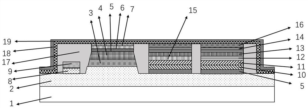
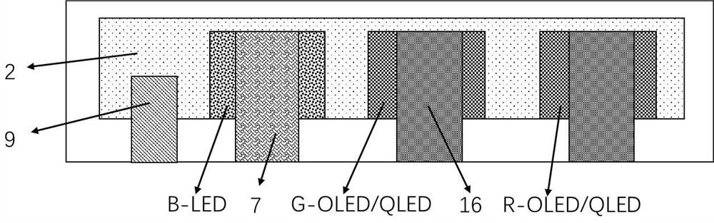
[0038] refer to figure 1 , the present invention provides an integrated package micro display chip, characterized in that it includes a substrate, a blue Micro-LED sub-pixel, a red Micro-OLED or Micro-QLED sub-pixel and a green Micro-OLED or Micro-QLED sub-pixel ; The n-electrode of the Micro-LED sub-pixel is connected to one of the electrodes of the Micro-OLED or Micro-QLED, the p-electrode of the Micro-LED sub-pixel, the other electrode of the red Micro-OLED or Micro-QLED, the green light The other electrode of the Micro-OLED or Micro-QLED is drawn out separately to form the lead-out electrodes of four integrated packaged micro-display chips. Micro-LED sub-pixels, red Micro-OLED or Micro-QLED sub-pixels and green Micro-OLED or Micro-QLED sub-pixels are integrated into a micro-display pixel with three-primary-color controllable light emission through ...


PUM


Abstract

The invention relates to an integrated packaging micro display chip, and the chip is characterized in that the chip comprises a substrate, a blue light Micro-LED sub-pixel, a red light Micro-OLED or Micro-QLED sub-pixel and a red light Micro-OLED or Micro-QLED sub-pixel; an n electrode of the Micro-LED sub-pixel is connected with one electrode of the Micro-OLED or the Micro-QLED, and a p electrode of the Micro-LED sub-pixel, the other electrode of the red light Micro-OLED or the Micro-QLED and the other electrode of the green light Micro-OLED or the Micro-QLED are respectively led out to form four leading-out electrodes of the integrated packaging micro-display chip. According to the invention, a blue light Micro-LED sub-pixel, a red light Micro-OLED or Micro-QLED sub-pixel, and a green light Micro-OLED or Micro-QLED sub-pixel are combined, and a micro-display pixel chip with a larger size and controllable luminescence of three primary colors is formed through wafer-level integration and packaging.

Description

technical field [0001] The invention relates to the field of photoelectric display technology, in particular to an integrated packaging micro-display chip and a preparation method thereof. Background technique [0002] Modern society has entered into informationization and is developing in the direction of intelligence. Display is the key link to realize information exchange and intelligence. Among the current display technologies, Micro-LED display technology is considered to be a disruptive next-generation display technology. Micro-LED display technology is a self-luminous display technology that integrates arrayed micron-scale LED light-emitting devices (μLEDs) on an active addressable drive substrate to achieve individual control and lighting to output display images. Micro-LED has the advantages of low power consumption (power consumption is only one-tenth of that of LCD), high brightness, high color saturation, high response speed, long life and high efficiency, and i...

Claims


Application Information

Patent Timeline
Patent Type & Authority Applications(China)
IPC IPC(8): H01L27/15H01L27/32H01L33/06H01L33/32H01L51/52
CPCH01L27/156H01L33/06H01L33/32H10K59/12H10K50/84
Inventor 周雄图阙思华郭太良张永爱吴朝兴林志贤严群叶芸
Owner FUZHOU UNIV
Why Eureka
Try Eureka