LED display module and LED display screen

A technology for display modules and circuits, applied in circuit shape/layout, instruments, electrical components, etc., can solve the problems of limited layout of driver ICs, not involving driver chip layout, limitations, etc., to optimize layout, reduce Production cost, the effect of reducing heat concentration

Pending Publication Date: 2021-08-27
江西省兆驰光电有限公司
View PDF3 Cites 1 Cited by
  • Summary
  • Abstract
  • Description
  • Claims
  • Application Information

AI Technical Summary

Problems solved by technology

Although this invention can solve the problems of short circuit and dead lights to a certain extent, it still cannot solve the problem of limited layout of driver ICs
[0004] In addition, an LED display module and its preparation method are disclosed in the description of the invention patent CN 202010175148.4, and a MINI LED mainboard manufacturing method is disclosed in the description of the invention patent CN 202010124562.2. There are some technical problems in the prior art, but none of them involve a solution to the limited layout of the driver chip

Method used


Image

  • LED display module and LED display screen
  • LED display module and LED display screen
  • LED display module and LED display screen

Examples


Embodiment 1

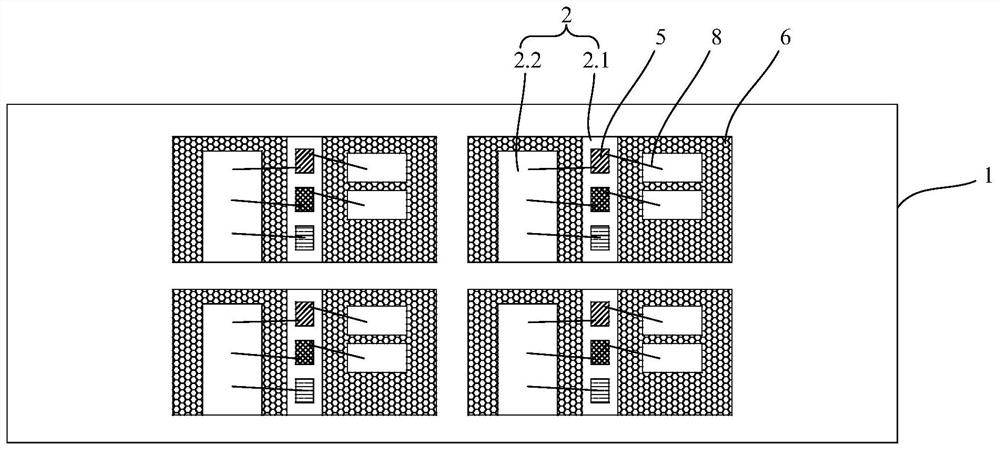
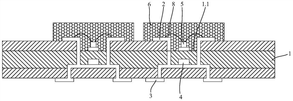
[0038] like figure 1 with figure 2 As shown, the structure of the LED display module of the present invention regarding the first embodiment. One of the LED display modules in the present invention includes a PCB substrate 1, and a front-side fixing provided with a front line 2 having a front line 2, and the back surface of the PCB substrate 1 is fixedly provided with a back line 3. The front lines 2 are The back line 3 is electrically connected, the PCB substrate 1 is fixedly provided with a drive chip 4, and the drive chip 4 is electrically connected to the front line 2 and the back line 3, and fixed settings on the PCB substrate 1 There is a light-emitting chipset 5, the light-emitting chipset 5 is electrically connected to the front line 2, and the PCB substrate 1 is also provided with encapsulation of the encapsulation of the light-emitting chipset 5 and the front line 2.

[0039] During the actual application, the lower side of each set of light-emitting chipset 5 is arrange...

Embodiment 2

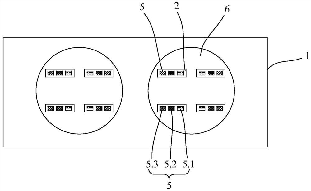
[0055] like image 3 with Figure 4 As shown, the structure of the LED display module of the present invention regarding the second embodiment. The present embodiment differs from the first embodiment in that each of the grooves 1.1 is equipped with a plurality of sets of light-emitting chip sets 5, and the plurality of sets of light-emitting chip sets 5 are flipped on the front line 2, and adjacent two The light-emitting chipset 5 is arranged between the light-emitting chipset 5 and the front lines 2 are in the groove 1.1. Specifically, the light-emitting chipset 5 is fixed to the front line 2 by tin or eutectic solder, each of which is electrically connected to a drive chip 4 through the front line 2.

[0056] Further, the light-emitting chipset 5 includes a red light chip 5.1, a green chip 5.2, and a blue chip 5.3, the red light chip 5.2, and the blue chip 5.3 are fixed to the solid crystal region 2.1, The red light chip 5.1, the green chip 5.2, and the blue chip 5.3 are fixed to...


PUM


Abstract

The invention relates to an LED display module and an LED display screen, the LED display module comprises a PCB substrate, the front surface of the PCB substrate is fixedly provided with a front surface circuit, the back surface of the PCB substrate is fixedly provided with a back surface circuit, the front surface circuit is electrically connected with the back surface circuit, a driving chip is fixedly arranged in the PCB substrate, and the driving chip is electrically connected with the front surface circuit and the back surface circuit. A light-emitting chip set is fixedly arranged on the PCB substrate, the light-emitting chip set is electrically connected with the front circuit, and packaging glue for packaging the light-emitting chip set and the front circuit is further arranged on the PCB substrate. Compared with the prior art, the layout of the LED display module is optimized, heat dissipation is accelerated, and cost is reduced.

Description

Technical field [0001] The present invention relates to the field of LED technology, in particular, in particular, to an LED display module and an LED display. Background technique [0002] The LED display module in the prior art is generally an LED light-emitting chip on one side of the PCB substrate, and is attached to the other side of the PCB substrate, and the connector is controlled by a drive chip, and the multi-set LED light-emitting chip is controlled. . However, even if a drive chip controls multiple sets of LED light-emitting chips, but because the LED light-emitting chip is arranged more and compact, especially small pitch LED display; driving chip size is large and requires good heat dissipation performance, so driving The layout space of the chip is very limited. [0003] A method of preparing a COB integrated plate and a lamp plate thereof, a display module thereof are disclosed in the specification of the invention patent CN 202010343182.8. Although the invention ...

Claims


Application Information

Patent Timeline
IPC IPC(8): H01L25/075H01L25/16H01L33/48H01L23/00H01L23/34H05K1/02G09F9/33
CPCG09F9/33H01L23/34H01L23/564H01L25/0753H01L25/167H01L33/483H05K1/02H05K2201/09
Inventor 刘传标杨春燕
Owner 江西省兆驰光电有限公司
Why Eureka
Try Eureka