Check patentability & draft patents in minutes with Patsnap Eureka AI!

TFT substrate and manufacturing method thereof

A manufacturing method and substrate technology, applied in semiconductor/solid-state device manufacturing, optics, instruments, etc., can solve problems such as Fogmura generation, and achieve the effect of reducing flow channels

Pending Publication Date: 2021-08-31
FUJIAN HUAJIACAI CO LTD
View PDF0 Cites 0 Cited by
  • Summary
  • Abstract
  • Description
  • Claims
  • Application Information

AI Technical Summary

Problems solved by technology

[0005] The technical problem to be solved by the present invention is: to provide a TFT substrate and its manufacturing method to solve the problem of Fog mura caused by polyimide not sticking to the substrate

Method used


Image

  • TFT substrate and manufacturing method thereof
  • TFT substrate and manufacturing method thereof

Examples


Embodiment 1

[0061] Please refer to figure 1 , Embodiment 1 of the present invention is:

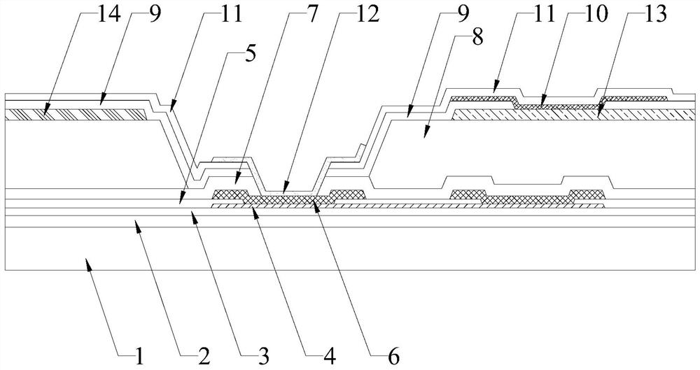
[0062] Please refer to figure 1 , a TFT substrate, comprising a glass substrate 1, on one side of the glass substrate 1, a gate metal layer 2, a gate insulating layer 3, an active layer 4, an etching stopper layer 5, a source and drain are sequentially stacked Metal layer 6, passivation layer 7, buffer layer 8, first insulating layer 9, common electrode layer 10 and second insulating layer 11, the first via hole is opened on the said etching barrier layer 5, and said first via hole A source-drain metal layer 6 is filled in the middle, a second via hole is opened on the passivation layer 7, a third via hole is opened on the first insulating layer 9, and a first via hole is opened on the second insulating layer 11. Four via holes, the second via hole, the third via hole and the fourth via hole are sequentially stacked and communicated, and the second via hole, the third via hole and the fourth via ho...

Embodiment 2

[0080] Please refer to figure 2 , the second embodiment of the present invention is:

[0081] A method for manufacturing a TFT substrate, comprising the steps of:

[0082] S1. Provide a glass substrate 1, the surface of the glass substrate 1 is covered with a gate metal layer 2;

[0083] S2, forming a gate insulating layer 3 and covering the surface of the gate metal layer 2;

[0084] S3, forming an active layer 4 and covering the surface of the gate insulating layer 3;

[0085] S4, forming an etching barrier layer 5, and covering the surface of the active layer 4; forming a first via hole in the etching barrier layer 5;

[0086] S5, forming the source-drain metal layer 6, and covering the surface of the etching barrier layer 5 and filling in the first via hole;

[0087] S6, forming a passivation layer 7 and covering the surface of the source-drain metal layer 6; forming a second via hole in the passivation layer 7;

[0088] S7, forming a buffer layer 8, and covering the...


PUM


Abstract

The invention relates to the technical field of TFT substrates, and especially relates to a TFT substrate and a manufacturing method thereof. The TFT substrate comprises a glass substrate, and a gate metal layer, a gate insulating layer, an active layer, an etching barrier layer, a source and drain metal layer, a passivation layer, a buffer layer, a first insulating layer, a common electrode layer and a second insulating layer are sequentially stacked on one side face of the glass substrate. The second metal layer is arranged between the first insulating layer and the buffer layer, the vertical cross section of the second metal layer is in a step shape, the step-shaped metal layer is designed on the buffer layer for guiding, and the step-shaped metal layer fixes a flowing channel of PI liquid, so that the flowing channel of the PI liquid is reduced, the PI liquid can be guided and diffused to an OC hole, THE PI can flow into the OC hole more easily, and the problem that Fog mura is generated due to the fact that the PI does not stick to the substrate is solved.

Description

technical field [0001] The invention relates to the technical field of TFT substrates, in particular to a TFT substrate and a manufacturing method thereof. Background technique [0002] In TFT-LCD (English full name is Thin Film Transistor Liquid Crystal Display, Thin Film Transistor Liquid Crystal Display), the alignment film coated on the CF substrate and TFT substrate plays a role in controlling the alignment direction of liquid crystal molecules. The TFT-LCD alignment film needs to have high mechanical strength and alignment memory function, and the alignment pattern must withstand a high temperature of nearly 200 degrees. Alignment film cannot react with liquid crystal. In engineering applications, polyimide (PI) can meet the above requirements at the same time. [0003] Alignment film requires alignment treatment to effectively control the arrangement of liquid crystal molecules. There are two main types of alignment technology: friction type and non-friction type. ...

Claims


Application Information

Patent Timeline
Patent Type & Authority Applications(China)
IPC IPC(8): H01L27/12H01L21/77G02F1/1362G02F1/1343
CPCG02F1/134363G02F1/1362G02F1/136227H01L27/124H01L27/1248H01L27/1259
Inventor 张桂瑜许汉东王强
Owner FUJIAN HUAJIACAI CO LTD
Features
  • R&D
  • Intellectual Property
  • Life Sciences
  • Materials
  • Tech Scout
  • Unparalleled Data Quality
  • Higher Quality Content
  • 60% Fewer Hallucinations
Learn More