Method for monitoring carrier concentration of SiGe structure

A technology of carrier concentration and concentration, which is applied in the direction of electrical components, semiconductor/solid-state device manufacturing, circuits, etc., to achieve the effects of improving monitoring frequency, high-frequency production line stability monitoring, and efficient monitoring

Pending Publication Date: 2021-09-07
SHANGHAI HUALI MICROELECTRONICS CORP
View PDF6 Cites 0 Cited by
  • Summary
  • Abstract
  • Description
  • Claims
  • Application Information

AI Technical Summary

Problems solved by technology

[0005] The purpose of the present invention is to provide a method for monitoring the carrier concentration of a SiGe structure to solve the above-mentioned problem of accurate, economical and efficient monitoring of the carrier concentration of a SiGe structure

Method used


Image

  • Method for monitoring carrier concentration of SiGe structure
  • Method for monitoring carrier concentration of SiGe structure
  • Method for monitoring carrier concentration of SiGe structure

Examples


Embodiment Construction

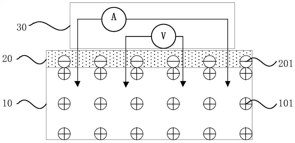
[0036] figure 1 Four Probe is a schematic diagram of a prior art SiGe structures. like figure 1 Shown, when using four-point probe tester 30 'of SiGe structures 10' of the resistivity testing, test results unstable, and there is a trend (latency) increased gradually with prolonged Q-time. And the inventors have found that instability results from the test wafer after removal of the monitoring machine growth, and gradually exposed to natural oxidation caused by air and the surface silicon atoms after the contact. Specifically, i.e. native oxide layer is SiGe 10 'hole carrier surface 101' formed on its surface structure 20 'dangling bonds charge 201' formed complex trapped charge, leading to increased resistivity, conductivity drops .

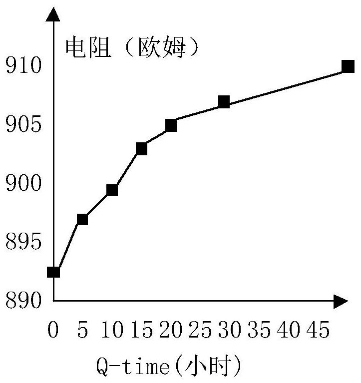
[0037] Meanwhile, data from the study of the inventors (e.g. figure 2 ) Found that a natural oxide 'has a very serious negative impact resistance test, SiGe structures 10' of the electrical resistivity SiGe structures 10 to almost linearly increased...


PUM

PropertyMeasurementUnit
thicknessaaaaaaaaaa

Abstract

The invention provides a method for monitoring the carrier concentration of a SiGe structure. The method comprises the following steps of: obtaining correlation data between the hole carrier concentration of a SiGe structure and the resistivity of the SiGe structure; providing a monitoring wafer, and forming a SiGe structure with P-type doped ions on the surface of the monitoring wafer by using a SiGe process corresponding to a product wafer; forming a barrier layer on the surface of the monitoring wafer, the barrier layer covering the SiGe structure; and obtaining the resistivity of the monitoring wafer, and obtaining the hole carrier concentration of the product wafer according to the correlation data. By forming the barrier layer on the surface of the SiGe structure, the change of the resistivity of the SiGe structure is slowed down, so that accurate, economical and efficient monitoring of the carrier concentration of the SiGe structure of the product wafer is realized; the specific hole carrier concentration can be obtained according to the obtained correlation data; and the monitoring method is simple and easy to implement, so that the monitoring frequency can be improved to realize high-frequency production line stability monitoring.

Description

Technical field [0001] The present invention relates to semiconductor technology, and particularly relates to a method for monitoring SiGe structures of the carrier concentration. Background technique [0002] With the rapid development of semiconductor technology, the size of the MOSFET devices continues to decrease, typically comprises a MOSFET device channel length is reduced, thinner gate oxide thickness, etc., to obtain a faster device speed. However, when the development of VLSI technology with deep sub-micron to, and particularly 28 nm technology node, the channel length is reduced it will bring a series of problems, such as reduced mobility of carriers, the device performance degradation, simply reducing the size of the device is difficult to meet the development of large scale integrated circuit technology. Whereby selective epitaxial grown SiGe technology to meet the needs of electrically PMOS 28nm or less by increasing the hole carrier mobility of the formed structure ...

Claims


Application Information

Patent Timeline
Patent Type & Authority Applications(China)
IPC IPC(8): H01L21/02H01L21/66
CPCH01L21/02532H01L21/0262H01L22/10H01L22/20
Inventor 李加昆杨奕刘猛
Owner SHANGHAI HUALI MICROELECTRONICS CORP
Why Eureka
Try Eureka