Wafer edge exposure method, wafer edge exposure device and mask plate

An edge exposure and mask technology, applied in the field of mask, wafer edge exposure device, wafer edge exposure, can solve the problems of effective wafer damage, affecting the quality of the wafer, etc., to reduce damage and ensure the exposure effect. Effect

Active Publication Date: 2021-09-24
CHANGXIN MEMORY TECH INC
View PDF6 Cites 0 Cited by
  • Summary
  • Abstract
  • Description
  • Claims
  • Application Information

AI Technical Summary

Problems solved by technology

[0003] However, the inventors of the present invention have found that the wafer edge exposure method in the prior art will cause damage to some effective wafers on the wafer edge, affecting the wafer quality

Method used


Image

  • Wafer edge exposure method, wafer edge exposure device and mask plate
  • Wafer edge exposure method, wafer edge exposure device and mask plate
  • Wafer edge exposure method, wafer edge exposure device and mask plate

Examples


Embodiment Construction

[0023] In order to make the object, technical solution and advantages of the present invention clearer, various embodiments of the present invention will be described in detail below in conjunction with the accompanying drawings. However, those of ordinary skill in the art can understand that, in each implementation manner of the present invention, many technical details are provided for readers to better understand the present application. However, even without these technical details and various changes and modifications based on the following implementation modes, the technical solution claimed in this application can also be realized.

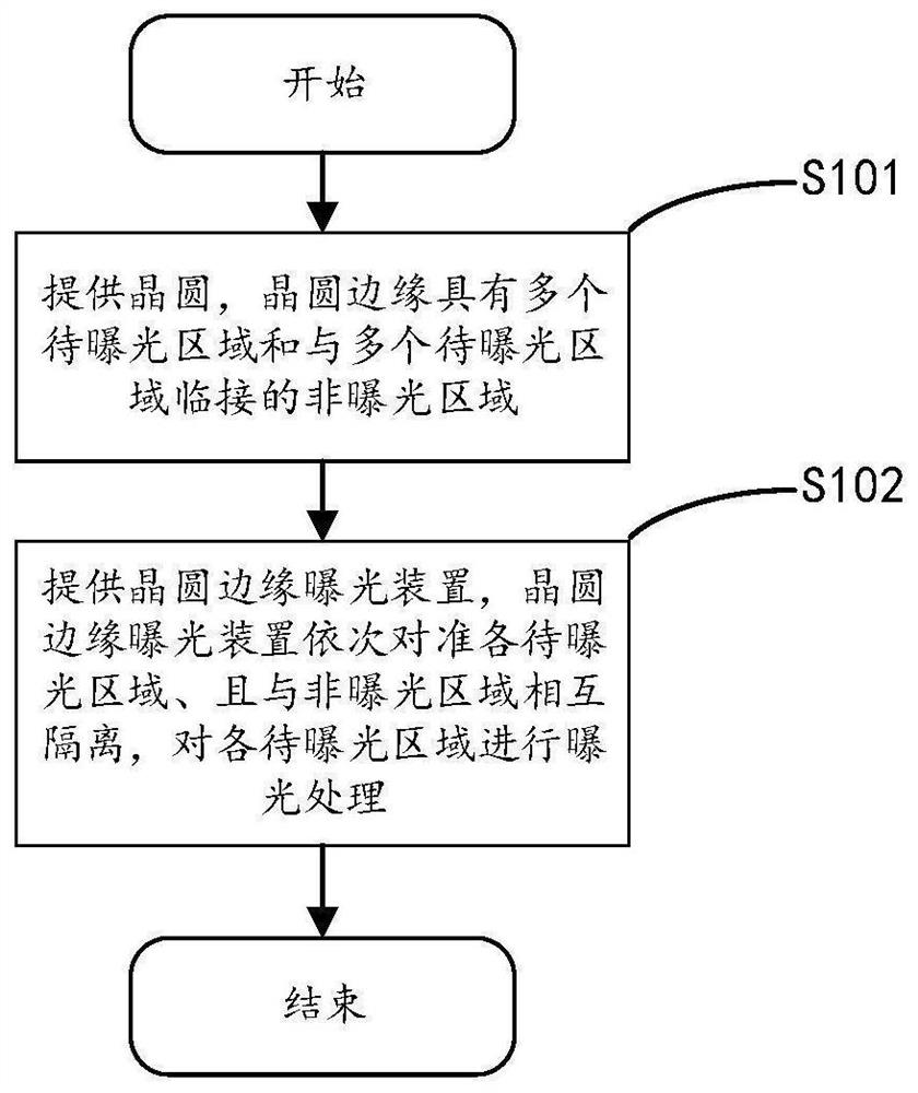
[0024] The first embodiment of the present invention relates to a wafer edge exposure method. The specific process is as figure 1 shown. Include the following steps:

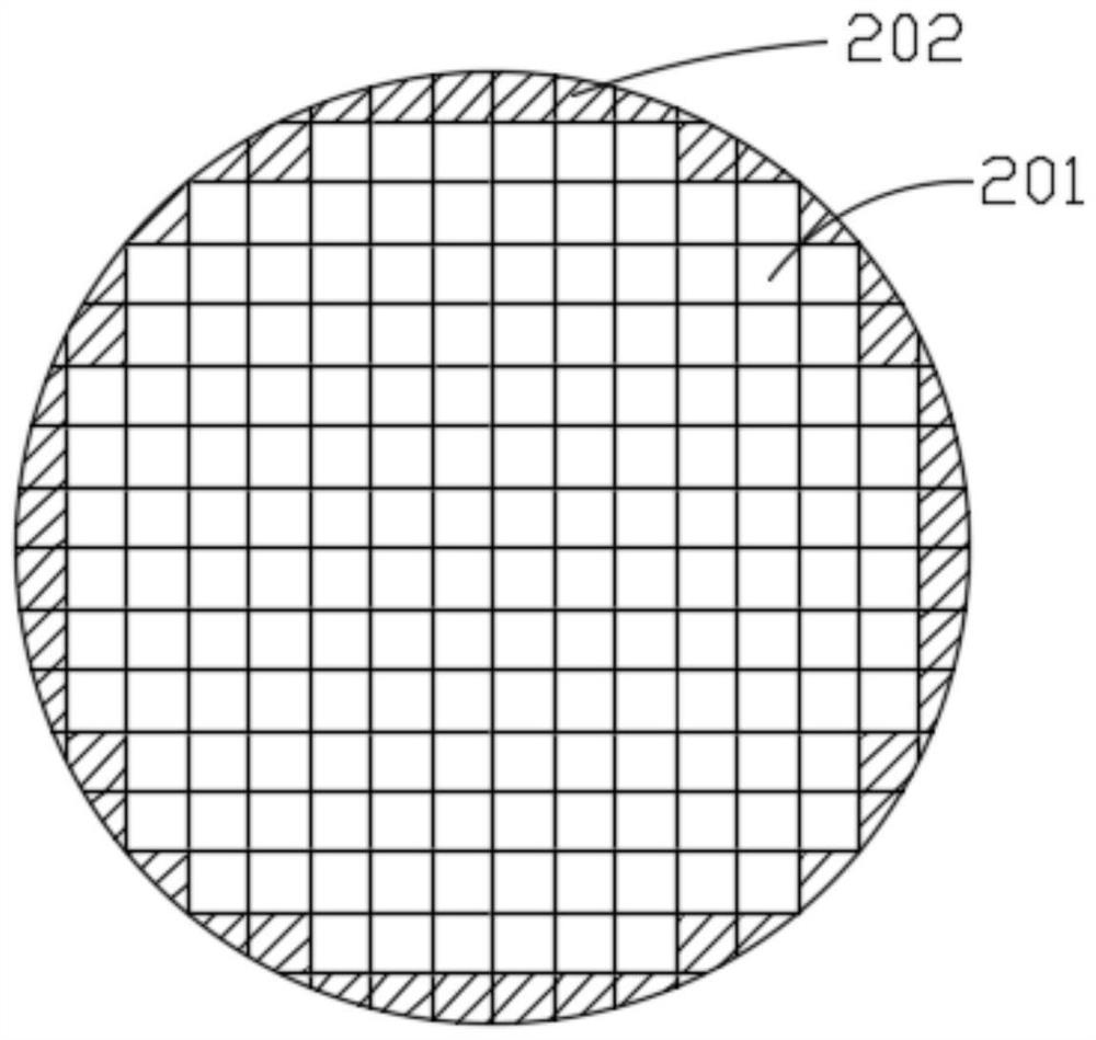
[0025] Step S101: providing a wafer, the edge of the wafer has a plurality of regions to be exposed and a non-exposed region adjacent to the regions to be exposed.

[002...


PUM


Abstract

The invention relates to the field of semiconductor manufacturing, and discloses a wafer edge exposure method, a wafer edge exposure device and a mask plate. The wafer edge exposure method comprises the steps that a wafer is provided, and the edge of the wafer is provided with a plurality of to-be-exposed areas and non-exposure areas adjacent to the to-be-exposed areas; a wafer edge exposure device is provided, the wafer edge exposure device is sequentially aligned with all the to-be-exposed areas and is isolated from the non-exposure areas, and exposure treatment is conducted on all the to-be-exposed areas. Compared with the prior art, the wafer edge exposure method, the wafer edge exposure device and the mask plate provided by the embodiment of the invention have the advantages that the damage to the effective wafer in the exposure process is reduced while the exposure effect of the wafer is ensured.

Description

technical field [0001] The invention relates to the field of semiconductor manufacturing, in particular to a wafer edge exposure method, a wafer edge exposure device and a mask plate. Background technique [0002] Wafer refers to the silicon wafer used in the production of silicon semiconductor integrated circuits. Because of its circular shape, it is called a wafer. It can be processed into various circuit element structures on silicon wafers, and become IC products with specific electrical functions. The raw material of the wafer is silicon, and there is an inexhaustible amount of silicon dioxide on the surface of the earth's crust. Silica ore is refined in an electric arc furnace, chlorinated with hydrochloric acid, and distilled to produce high-purity polysilicon. However, the traditional wafer production process varies from good to bad, and generally has the disadvantages of cumbersome process, high cost, and low yield rate. In the prior art, in order to improve the ...

Claims


Application Information

Patent Timeline
Patent Type & Authority Applications(China)
IPC IPC(8): G03F7/20G03F9/00G03F1/54
CPCG03F7/2022G03F9/7073G03F1/54
Inventor 陈琦南
Owner CHANGXIN MEMORY TECH INC
Why Eureka
Try Eureka