Semiconductor packaging method

A packaging method and semiconductor technology, applied in semiconductor/solid-state device manufacturing, electrical components, circuits, etc., can solve the problems of poor electrical connection between the redistribution layer and the pads of the chip, failure of packaging products, and chip movement. Guarantee the effect of electrical connection, not easy to move, and improve the yield

Pending Publication Date: 2021-09-24
SIPLP MICROELECTRONICS CHONGQING CO LTD
View PDF10 Cites 1 Cited by
  • Summary
  • Abstract
  • Description
  • Claims
  • Application Information

AI Technical Summary

Problems solved by technology

[0003] In the existing chip packaging technology, in the process of forming the encapsulation layer, the chip may be moved, which may lead to poor electrical connection between the subsequent rewiring layer and the pads of the chip, resulting in the final packaged product fail

Method used


Image

  • Semiconductor packaging method
  • Semiconductor packaging method
  • Semiconductor packaging method

Examples


Embodiment Construction

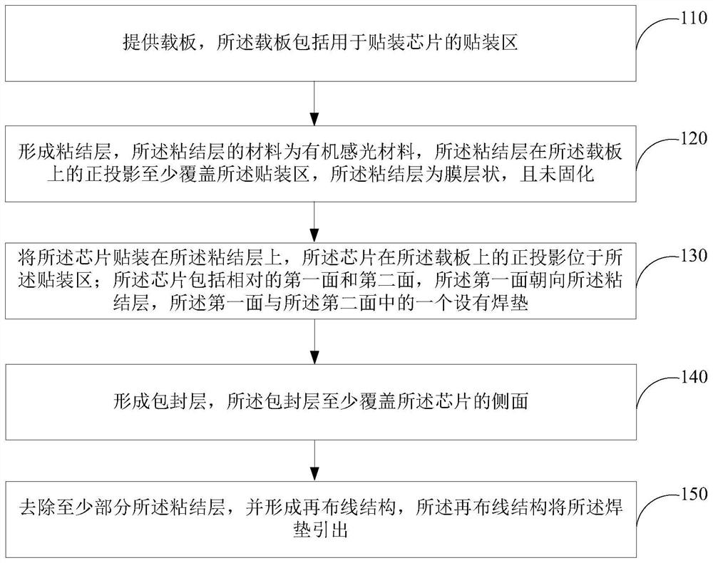
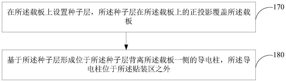
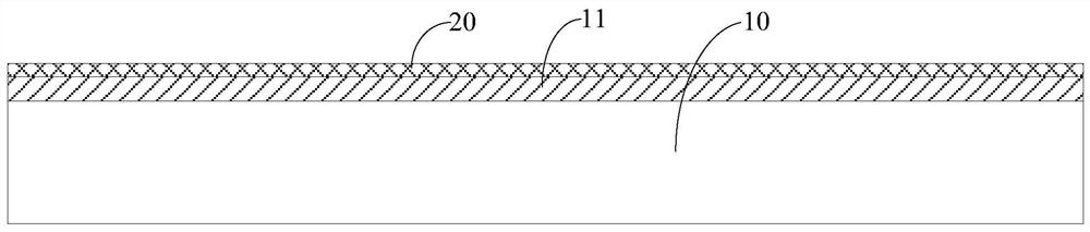
[0054] Reference will now be made in detail to the exemplary embodiments, examples of which are illustrated in the accompanying drawings. When the following description refers to the accompanying drawings, the same numerals in different drawings refer to the same or similar elements unless otherwise indicated. The embodiments described in the following exemplary embodiments do not represent all embodiments consistent with the present application. Rather, they are merely examples of apparatuses and methods consistent with aspects of the present application as recited in the appended claims.

[0055]The terminology used in this application is for the purpose of describing particular embodiments only, and is not intended to limit the application. As used in this application and the appended claims, the singular forms "a", "the", and "the" are intended to include the plural forms as well, unless the context clearly dictates otherwise. It should also be understood that the term "...


PUM

PropertyMeasurementUnit
thicknessaaaaaaaaaa
thicknessaaaaaaaaaa
thicknessaaaaaaaaaa

Abstract

The invention provides a semiconductor packaging method. The semiconductor packaging method comprises the following steps: providing a carrier plate, wherein the carrier plate comprises a mounting area for mounting a chip; forming a bonding layer, wherein the material of the bonding layer is an organic photosensitive material, the orthographic projection of the bonding layer on the carrier plate at least covers the mounting area, and the bonding layer is in a film layer shape and is not cured; mounting the chip on the bonding layer, wherein the orthographic projection of the chip on the carrier plate is located in the mounting area, wherein the chip comprises a first surface and a second surface which are opposite to each other, the first surface faces the bonding layer, and one of the first surface and the second surface is provided with a welding pad; forming an encapsulation layer, wherein the encapsulation layer at least covers the side surface of the chip; and removing at least part of the bonding layer, forming a rewiring structure, and leading out the welding pad through the rewiring structure.

Description

technical field [0001] The present application relates to the technical field of semiconductors, in particular to a semiconductor packaging method. Background technique [0002] Common semiconductor packaging technology, such as chip packaging technology, mainly includes the following process: firstly, the chip is mounted on the carrier board, heat-pressed and molded to form an encapsulation layer, the carrier board is peeled off, and then the bonding pad of the chip is formed. rewiring layer. [0003] In the existing chip packaging technology, in the process of forming the encapsulation layer, the chip may be moved, which may lead to poor electrical connection between the subsequent rewiring layer and the pads of the chip, resulting in the final packaged product invalidated. Contents of the invention [0004] The embodiment of the present application provides a semiconductor packaging method. The semiconductor packaging method includes: [0005] providing a carrier bo...

Claims


Application Information

Patent Timeline
Patent Type & Authority Applications(China)
IPC IPC(8): H01L21/56H01L21/48
CPCH01L21/563H01L21/568H01L21/4821
Inventor 杨威源
Owner SIPLP MICROELECTRONICS CHONGQING CO LTD
Why Eureka
Try Eureka