
Stacked photonic iii-v semi-conductor device

A III-V, semiconductor technology, applied in the field of stacked photonic III-V semiconductor devices, can solve problems such as residual current leakage current

Active Publication Date: 2021-09-24
AZUR SPACE SOLAR POWER
View PDF16 Cites 0 Cited by
  • Summary
  • Abstract
  • Description
  • Claims
  • Application Information

AI Technical Summary

Problems solved by technology

[0012] A disadvantage of the described structure is the residual or leakage current that occurs during operation in the cut-off direction especially at the edges of flat pn junctions or mesa structures

Method used


Image

  • Stacked photonic iii-v semi-conductor device
  • Stacked photonic iii-v semi-conductor device
  • Stacked photonic iii-v semi-conductor device

Examples


Embodiment Construction

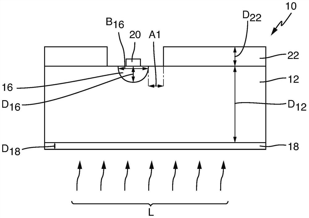
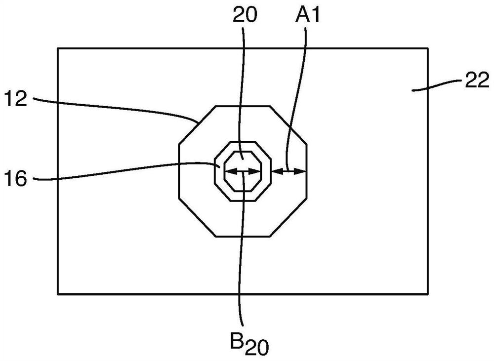
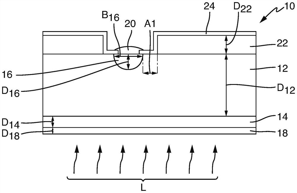
[0105] figure 1 The image in the figure shows a stacked photonic III-V semiconductor device 10 having an absorbing region 12, a highly doped first semiconductor contact region 16 and having a first metal connection layer 18, a second metal connection connection Layer 20 and III-V semiconductor passivation layer 22.

[0106] The absorption region 12 is doped with a second conductivity type with 8·10 11 cm -3 to 5·10 14 cm -3 A dopant at a low to very low dopant concentration, and has a first lattice constant and a layer thickness D12 of at least 80 μm (eg, 100 μm or 1000 μm).

[0107] On the underside of the absorption region 12 , a first metal connection layer 18 as a thin planar layer with a layer thickness D18 of up to 2 μm (eg 10 nm) follows in a material-bonding manner. metal layer. Alternatively (not shown), the metal connection layer 18 is configured in the form of strips or fingers or points.

[0108] The highly doped first semiconductor contact region 16 is of t...


PUM


Abstract

A stacked photonic III-V semiconductor device has a second metallic connection contact layer at least formed in regions, a highly doped first semiconductor contact region of a first conductivity type, a very low doped absorption region of the first or second conductivity type having a layer thickness of 20 [mu]m-2000 [mu]m, a first metallic connection contact layer at least formed in regions, wherein the first semiconductor contact region extends into the absorption region in a trough shape, the second metallic connection contact layer is integrally bonded to the first semiconductor contact region and the first metallic connection contact layer is arranged below the absorption region. In addition, the stacked photonic III-V semiconductor device has a doped III-V semiconductor passivation layer of the first or second conductivity type, wherein the III-V semiconductor passivation layer is arranged at the upper side of the absorption region at a first distance of at least 10 [mu]m to the first semiconductor contact region.

Description

technical field [0001] The invention relates to a stacked photonic (photonisch) III-V semiconductor device. Background technique [0002] III-V semiconductor diodes are used in the respective fields with adapted parameters during this time. [0003] From "GaAs Power Devices" of Ashkinazi in Germany, ISBN 965-7094-19-4, in the 8th and 9th pages, it is known that a kind of + -n-n + High voltage semiconductor devices made of GaAs. [0004] Other high-voltage-resistant III-V semiconductor devices and corresponding manufacturing methods are also from documents DE 10 2016 013 540 A1, DE 10 2016 013 541 A1, DE 10 2016 015 056 A1, DE 10 2017 002 935 A1 and DE10 2017 002 936 A1 known in. [0005] III-V semiconductor devices are also used in 2D pixel array detectors as pixels or semiconductor detectors. [0006] Infrared detectors are known, for example, from Barton et al., "InGaAs NIR focal plane arrays forimaging and DWDM applications", Infrared Detectors and Focal Plane Arrays...

Claims


Application Information

Patent Timeline
Patent Type & Authority Applications(China)
IPC IPC(8): H01L31/0352H01L31/0216H01L31/0304H01L31/103
CPCH01L31/03046H01L31/02161H01L31/1035H01L31/035281H01L29/8611H01L29/20H01L29/205H01L29/0657H01L29/402H01L29/66204H01L29/04H01L31/0735H01L31/0304Y02E10/544H01L31/03042H01L31/0336H01L31/118
Inventor G·施特罗布尔
Owner AZUR SPACE SOLAR POWER
Learn More