Photoelectric device

A technology of optoelectronic devices and optoelectronic materials, applied in instruments, optics, nonlinear optics, etc., can solve the problem of large light propagation loss and achieve the effect of suppressing propagation loss

Pending Publication Date: 2021-10-01
TDK CORPARATION
View PDF3 Cites 0 Cited by
  • Summary
  • Abstract
  • Description
  • Claims
  • Application Information

AI Technical Summary

Problems solved by technology

High-speed optical modulators of 40Gb / s or higher are commercialized, but there is a big disadvantage that the total length is about 10cm
However, the cross-sectional shape of the optical waveguides 22a, 22b is rectangular, and the propagation loss of light is relatively large.

Method used


Image

  • Photoelectric device
  • Photoelectric device
  • Photoelectric device

Examples


Embodiment Construction

[0028] Hereinafter, modes for implementing the present invention will be described in detail with reference to the drawings.

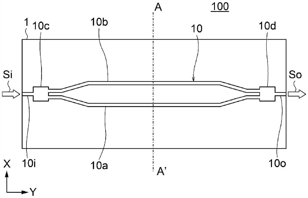
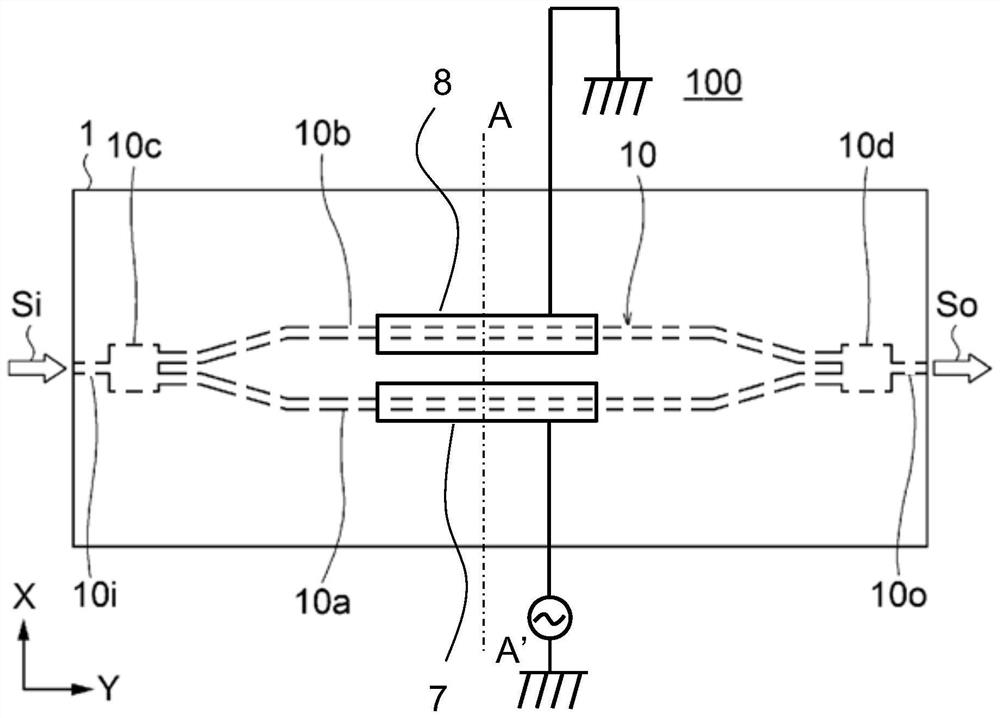
[0029] Fig. 1 (a) and Fig. 1 (b) are the top view of the optical modulator (optoelectronic device) 100 of an embodiment of the present invention, Fig. 1 (a) only shows the optical waveguide, Fig. 1 (b) shows The electrode of the light modulator 100 is the whole of the light modulator 100 .

[0030] As shown in FIG. 1(a) and FIG. 1(b), the optical modulator 100 includes: a Mach-Zehnder optical waveguide 10 having first and second optical waveguides 10a formed on a substrate 1 and arranged parallel to each other, 10b; the first electrode 7 provided along the first optical waveguide 10a; the second electrode 8 provided along the second optical waveguide 10b.

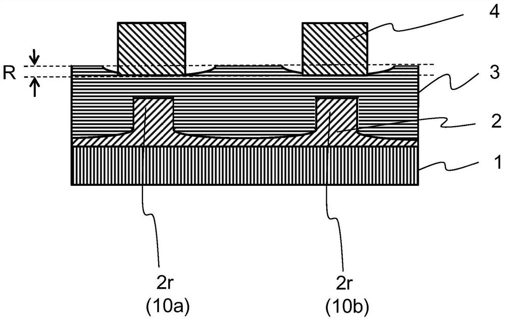
[0031] The Mach-Zehnder optical waveguide 10 is an optical waveguide having a structure of a Mach-Zehnder interferometer. It has first and second optical waveguides 10a and 10b branched from one i...


PUM


Abstract

The invention provides a photoelectric device comprising: a substrate; an optical waveguide composed of a photoelectric material film formed in a ridge shape on the substrate; a buffer layer provided so as to cover the optical waveguide; and an upper electrode arranged on the optical waveguide via the buffer layer, wherein the buffer layer has a recess on the upper electrode side of the optical waveguide. According to the photoelectric device provided by the invention, the propagation loss of light can be suppressed.

Description

technical field [0001] The invention relates to an optoelectronic device used in the fields of optical communication and optical measurement. Background technique [0002] With the popularity of the Internet, the communication volume has increased dramatically, and the importance of optical fiber communication is very high. Optical fiber communication is a communication method that converts electrical signals into optical signals and transmits optical signals through optical fibers. It has the characteristics of wide bandwidth, low loss, and strong noise immunity. [0003] Due to such advantages, optical fiber communication is applied to various products, and optical switching devices and optical modulators are examples thereof. In particular, a direct modulation method using a semiconductor laser and an external modulation method using an optical modulator are known as methods in which an optical modulation device converts an electrical signal into an optical signal. Alth...

Claims


Application Information

Patent Timeline
IPC IPC(8): G02F1/035G02F1/03
CPCG02F1/035G02F1/0305G02F1/03G02F1/212G02F1/0316G02F2201/07
Inventor 长瀬健司田家裕宫田晋吾
Owner TDK CORPARATION
Why Eureka
Try Eureka