Semiconductor memory device

A storage device and semiconductor technology, applied in semiconductor devices, electric solid state devices, electrical components, etc., can solve problems such as inability to meet product requirements

Pending Publication Date: 2021-10-01
FUJIAN JINHUA INTEGRATED CIRCUIT CO LTD
View PDF5 Cites 0 Cited by
  • Summary
  • Abstract
  • Description
  • Claims
  • Application Information

AI Technical Summary

Problems solved by technology

Generally speaking, the active area is a plurality of patterns formed on the substrate by photolithography, etching and other manufacturing processes. T...

Method used


Image

  • Semiconductor memory device
  • Semiconductor memory device
  • Semiconductor memory device

Examples


Embodiment Construction

[0039] In order to enable those who are familiar with the technical field of the present invention to further understand the present invention, several preferred embodiments of the present invention are enumerated below, and in conjunction with the accompanying drawings, the constitutional content and intended achievement of the present invention are explained in detail. effect. Those skilled in the art of the present invention can refer to the following embodiments without departing from the spirit of the present invention, and replace, reorganize, and mix features in several different embodiments to complete other embodiments.

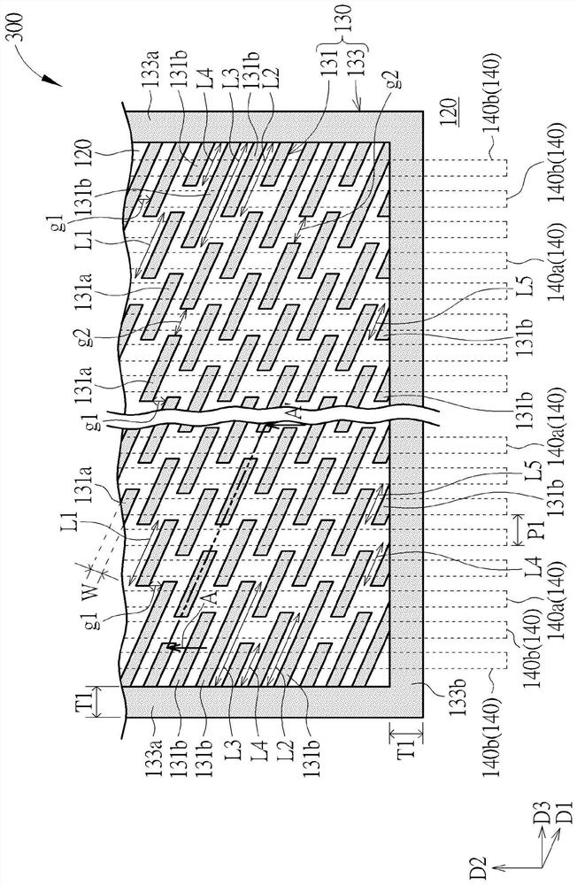
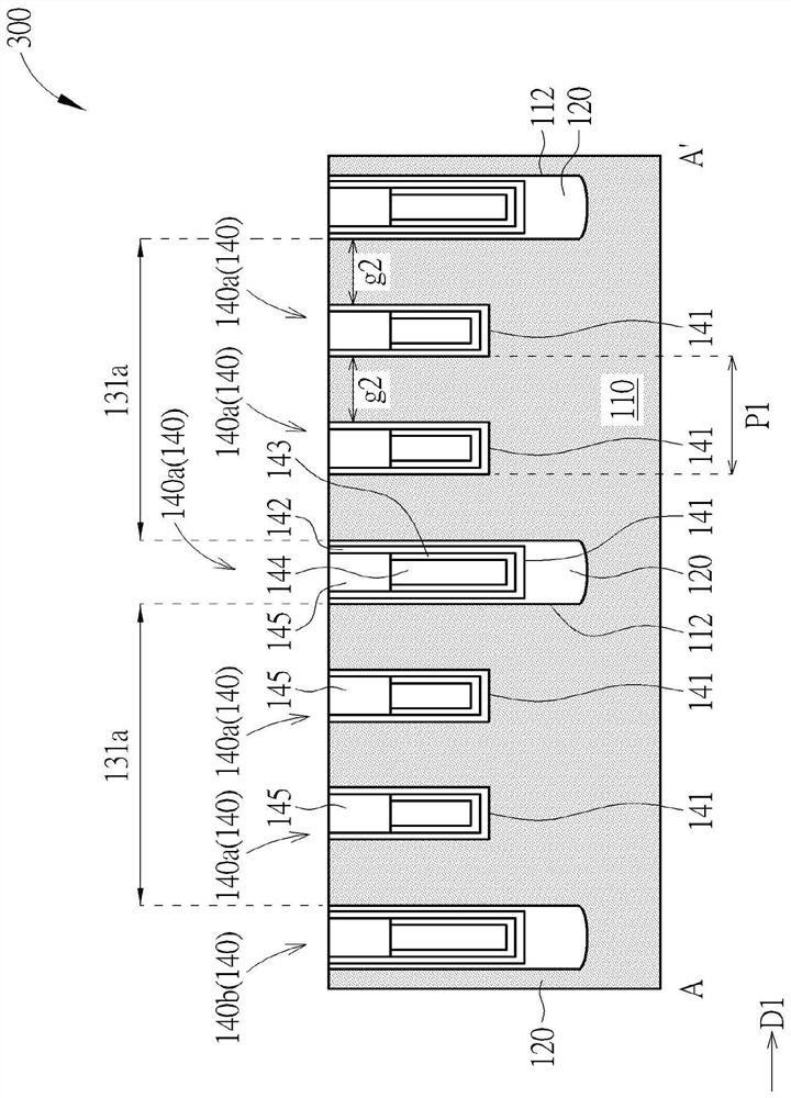
[0040] Please refer to Figure 1 to Figure 2 , which is a schematic diagram of the manufacturing process of the semiconductor storage device 300 in the preferred embodiment of the present invention, wherein, figure 1 as well as figure 2 They are respectively a schematic top view and a schematic cross-sectional view of the semiconductor storage dev...


PUM


Abstract

A semiconductor memory device includes a substrate, an active structure, a shallow trench isolation, and a plurality of word lines. The active structure is arranged in the substrate and comprises a plurality of first active segments and a plurality of second active segments, each first active segment and each second active segment extend towards a first direction in parallel, and the second active segments are arranged on the outer sides of all the first active segments. The shallow trench isolation is arranged in the substrate, surrounds the active structure and comprises a plurality of first parts and a plurality of second parts. The word lines extend in parallel along a second direction and are disposed in the substrate. At least two of the word lines are interleaved with only the second active segments, or at least one of the word lines does not pass through any second portion. Therefore, direct conduction between the word lines and bit lines can be effectively avoided.

Description

technical field [0001] The invention relates to a semiconductor storage device, in particular to a semiconductor storage device including an active structure and shallow trench isolation. Background technique [0002] With the miniaturization of semiconductor devices and the complexity of integrated circuits, the size of components is continuously reduced and the structure is also constantly changing. Therefore, maintaining the performance of small-sized semiconductor components is currently the main goal of the industry. In the semiconductor manufacturing process, it is mostly based on defining a plurality of active regions on the substrate, and then forming required components on the active regions. Generally speaking, the active area is a plurality of patterns formed on the substrate by photolithography, etching and other manufacturing processes. The pitch is also gradually shrinking, making its manufacturing process also face many restrictions and challenges, so that it...

Claims


Application Information

Patent Timeline
IPC IPC(8): H01L27/02H01L27/115
CPCH01L27/0203H01L27/0207H10B69/00
Inventor 张钦福童宇诚
Owner FUJIAN JINHUA INTEGRATED CIRCUIT CO LTD
Why Eureka
Try Eureka