Semiconductor device and forming method thereof

A semiconductor and conductor layer technology, which is applied in semiconductor devices, semiconductor/solid-state device manufacturing, transistors, etc., and can solve the problems of increased manufacturing process and design difficulty and complexity.

Pending Publication Date: 2022-06-21
FUJIAN JINHUA INTEGRATED CIRCUIT CO LTD
View PDF0 Cites 0 Cited by
  • Summary
  • Abstract
  • Description
  • Claims
  • Application Information

AI Technical Summary

Problems solved by technology

In response to product demand, the density of memory cells in the array area must continue to increa

Method used


Image

  • Semiconductor device and forming method thereof
  • Semiconductor device and forming method thereof
  • Semiconductor device and forming method thereof

Examples


Embodiment Construction

[0066] In order to enable those skilled in the art to which the present invention pertains to further understand the present invention, the preferred embodiments of the present invention are specifically listed below, together with the accompanying drawings, to describe in detail the composition of the present invention and what it wants to achieve. effect. It should be noted that, in the following embodiments, other embodiments can be completed by substituting, recombining, and mixing features in several different embodiments without departing from the spirit of the present invention.

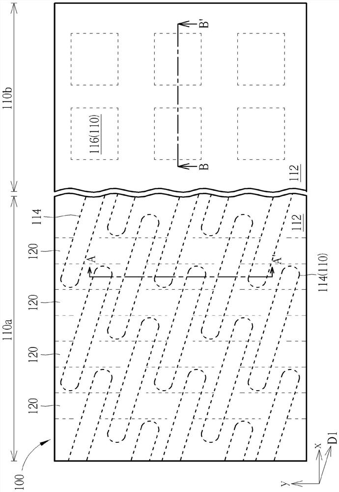
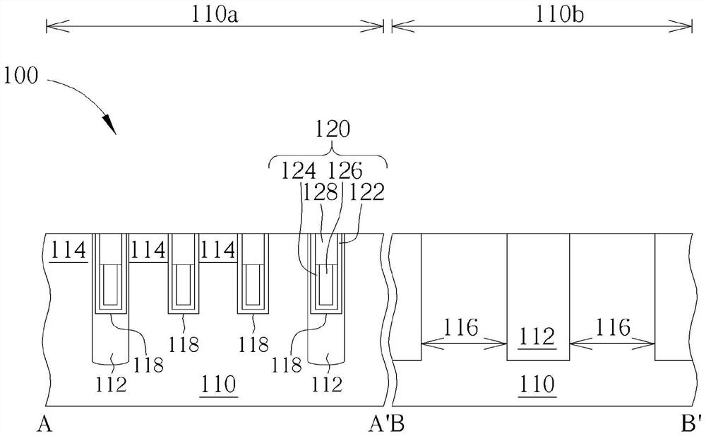
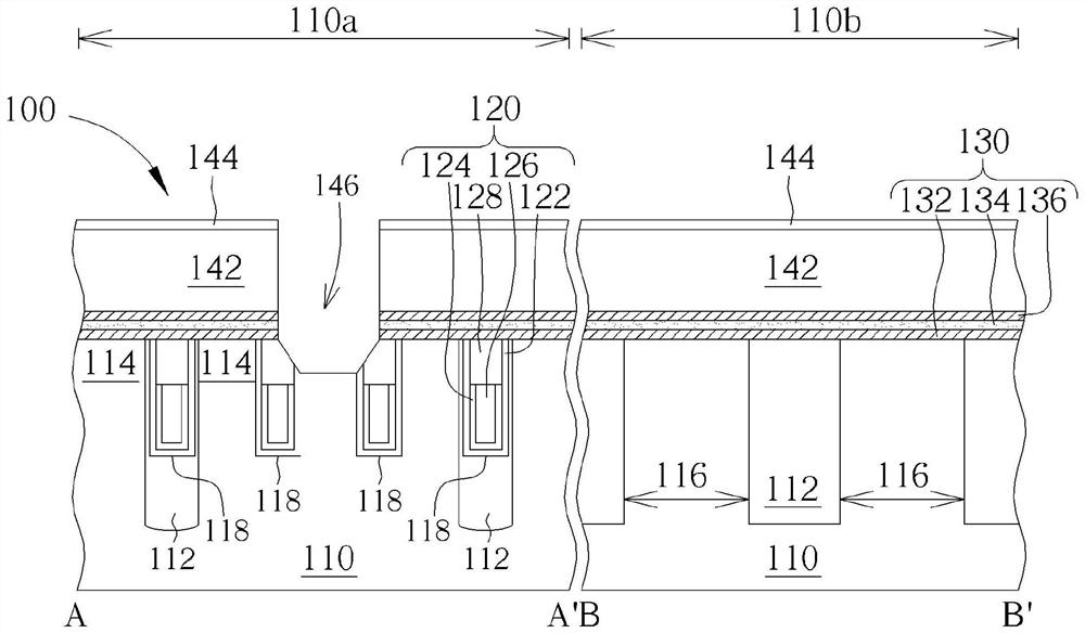
[0067] Please refer to Figure 1 to Figure 5 , which is a schematic diagram of the steps of the formation method of the semiconductor device 100 in the first embodiment of the present invention, wherein, figure 1 It is a schematic top view of the semiconductor device 100 in the formation stage, Figure 2 to Figure 5 It is a schematic cross-sectional view of the semiconductor device 100 at di...


PUM


Abstract

The invention discloses a semiconductor device and a forming method thereof. The semiconductor device comprises a substrate, a plurality of bit lines, a plurality of bit line contacts, a gate structure, a first oxidation interface layer and a second oxidation interface layer. The bit lines are arranged on the substrate, and the bit line contacts are located below part of the bit lines. The gate structure is arranged on the substrate, and the bit line and the gate structure respectively comprise a semiconductor layer, a barrier layer, a conductive layer and a cover layer which are stacked in sequence. The first oxidation interface layer is disposed between the bit line contact and the semiconductor layer of the bit line. The second oxidation interface layer is arranged in the semiconductor layer of the gate electrode, and the topmost surface of the first oxidation interface layer is higher than the topmost surface of the second oxidation interface layer. Therefore, the bit line and the bit line contact can have better structural reliability, so that the semiconductor device can achieve more optimized component efficiency.

Description

technical field [0001] The present invention relates to a semiconductor device and a method for forming the same, particularly a semiconductor memory device and a method for forming the same. Background technique [0002] With the development trend of various electronic products toward miniaturization, the design of semiconductor memory devices must also meet the requirements of high integration and high density. For a dynamic random access memory (DRAM) with a recessed gate structure, it can obtain a longer carrier channel length in the same semiconductor substrate, so as to reduce the leakage of the capacitor structure. Therefore, under the current mainstream development trend, it has gradually replaced the dynamic random access memory with only a planar gate structure. [0003] Generally speaking, a DRAM with a recessed gate structure is composed of a large number of memory cells gathered to form an array area for storing information, and each memory cell can be composed...

Claims


Application Information

Patent Timeline
IPC IPC(8): H01L27/108H01L21/8242
CPCH10B12/312H10B12/34H10B12/482
Inventor 永井享浩
Owner FUJIAN JINHUA INTEGRATED CIRCUIT CO LTD
Why Eureka
Try Eureka