Laser device chip positioning and clamping mechanism

A clamping mechanism and laser technology, applied in lasers, laser parts, semiconductor lasers, etc., can solve the problems of foveated folds, easy to be stressed and affected, etc.

Inactive Publication Date: 2021-10-01
深圳市君康源智能科技有限公司
View PDF0 Cites 0 Cited by
  • Summary
  • Abstract
  • Description
  • Claims
  • Application Information

AI Technical Summary

Problems solved by technology

[0003] When the current laser chip positioning and clamping mechanism fixes the chip, there are many transistors inside the chip, and its material is relatively fragile and easily deformed by external force. After the center is fixed, both sides of the chip are more likely to be stressed, and the center There will be concave folds, and the inside of the chip will be damaged. It is difficult for the conventional fixed clamping mechanism to quickly cooperate with the equipment for processing, and the production efficiency of the chip is slow. When the chip is processed in multiple places, the remaining materials from the previous processing will remain. On its surface, it affects the quality of later products, and the later clamping will be adversely affected at the same time. Therefore, we propose a laser chip positioning and clamping mechanism

Method used


Image

  • Laser device chip positioning and clamping mechanism
  • Laser device chip positioning and clamping mechanism
  • Laser device chip positioning and clamping mechanism

Examples


Embodiment 1

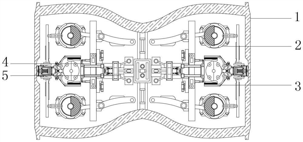
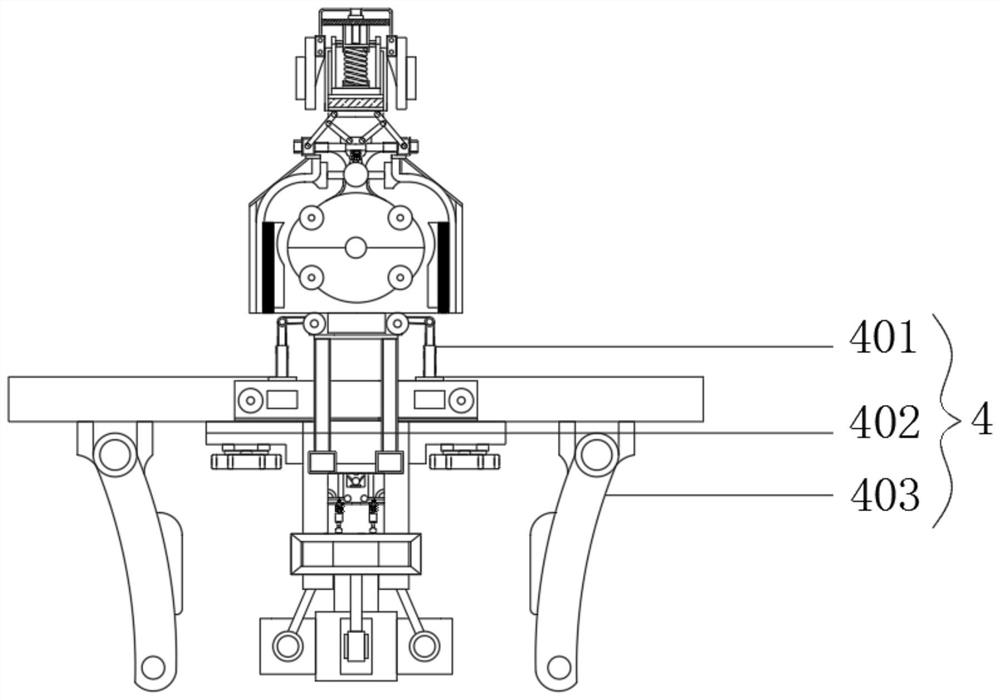
[0022] see Figure 1-5 , a laser chip positioning and clamping mechanism, including a chip positioning and clamping mechanism, the chip positioning and clamping mechanism includes a main clamping frame 5, the inner center of the main clamping frame 5 is movably connected with a fixed slide bar 504, the The left and right sides of the fixed slide bar 504 are movably connected with a curved clamping rod 403, and the outside of the curved clamping rod 403 is movably connected with a clamping rod frame 4, and the left and right sides of the clamping rod frame 4 Both are movably connected with a curved fit frame 304, and the outside of the curved fit frame 304 is movably connected with a stress buffer frame 3, and the upper and lower sides of the stress buffer frame 3 are movably connected with a connecting rod 201. The outer side of the bar 201 is movably connected with a distance-adjustable wheel frame 2 .

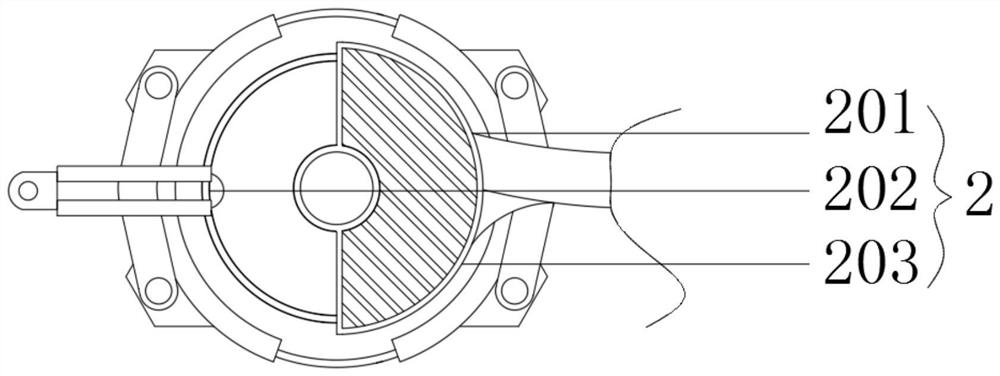
[0023] Further, the distance adjusting wheel frame 2 includes a connect...

Embodiment 2

[0027] see figure 1 and Figure 4 , a laser chip positioning and clamping mechanism, including a chip positioning and clamping mechanism, the chip positioning and clamping mechanism includes a main clamping frame 5, the inner center of the main clamping frame 5 is movably connected with a fixed slide bar 504, the The left and right sides of the fixed slide bar 504 are movably connected with a curved clamping rod 403, and the outside of the curved clamping rod 403 is movably connected with a clamping rod frame 4, and the left and right sides of the clamping rod frame 4 Both are movably connected with a curved fit frame 304, and the outside of the curved fit frame 304 is movably connected with a stress buffer frame 3, and the upper and lower sides of the stress buffer frame 3 are movably connected with a connecting rod 201. The outer side of the bar 201 is movably connected with a distance-adjustable wheel frame 2 .

[0028] Further, the main clamping frame 5 includes a lower ...

Embodiment 3

[0032] see figure 1 and Figure 5 , a laser chip positioning and clamping mechanism, including a chip positioning and clamping mechanism, the chip positioning and clamping mechanism includes a main clamping frame 5, the inner center of the main clamping frame 5 is movably connected with a fixed slide bar 504, the The left and right sides of the fixed slide bar 504 are movably connected with a curved clamping rod 403, and the outside of the curved clamping rod 403 is movably connected with a clamping rod frame 4, and the left and right sides of the clamping rod frame 4 Both are movably connected with a curved fit frame 304, and the outside of the curved fit frame 304 is movably connected with a stress buffer frame 3, and the upper and lower sides of the stress buffer frame 3 are movably connected with a connecting rod 201. The outer side of the bar 201 is movably connected with a distance-adjustable wheel frame 2 .

[0033] Further, the stress buffer frame 3 includes a torsio...


PUM


Abstract

The invention relates to the technical field of chip manufacturing, and provides a laser device chip positioning and clamping mechanism, which comprises a chip positioning and clamping mechanism body, wherein the chip positioning and clamping mechanism body comprises a main clamping frame, a fixed sliding rod is movably connected to the center of the inner side of the main clamping frame, and curved clamping rods are movably connected to the left side and the right side of the fixed sliding rod. According to the laser device chip positioning and clamping mechanism, the curved matching frame drives the extrusion air bag to extrude towards the center, at the moment, chip machining is in the later stage, the surface of the chip has many processing residues, the extrusion air bag extrudes the telescopic rods on the two sides of the extrusion frame in a linkage mode to move towards the inner side, the telescopic rods extrude the pushing frame to move towards the inner side, and the pushing frame pushes the processing material on the surface of the chip to push the processing material out of the normal processing range of the chip, so that the residual material in the previous processing is prevented from being left on the surface of the chip, the quality of a later product is improved, and the later clamping is not influenced.

Description

technical field [0001] The invention relates to the technical field of chip production, in particular to a laser chip positioning and clamping mechanism. Background technique [0002] A chip is a kind of integrated circuit. With the development of the times, integrated circuits have become ubiquitous. Computers, mobile phones and other digital appliances have become an indispensable part of the modern social structure. During processing, it is necessary to use a positioning and clamping mechanism to fix it, so as to improve the production efficiency of chips. [0003] When the current laser chip positioning and clamping mechanism fixes the chip, there are many transistors inside the chip, and its material is relatively fragile and easily deformed by external force. After the center is fixed, both sides of the chip are more likely to be stressed, and the center There will be concave folds, and the inside of the chip will be damaged. It is difficult for the conventional fixed...

Claims


Application Information

Patent Timeline
Patent Type & Authority Applications(China)
IPC IPC(8): H01S5/02365H01S5/02375
CPCH01S5/02365H01S5/02375
Inventor 郑君雄郑世进崔雨舟王青
Owner 深圳市君康源智能科技有限公司
Why Eureka
Try Eureka