Printed circuit board etching device and method

A technology for printed circuit boards and etching devices, which is applied to printed circuits, printed circuit manufacturing, and removal of conductive materials by chemical/electrolytic methods, and can solve problems such as inability to etch circuit boards and inability to etch

Inactive Publication Date: 2021-10-01
山西汇诚晋海科技有限公司
View PDF0 Cites 3 Cited by
  • Summary
  • Abstract
  • Description
  • Claims
  • Application Information

AI Technical Summary

Problems solved by technology

During the etching process, the clamped part of the circuit board is blocked by the fixture, and the etching solution cannot etch the part, and the circuit board cannot be etched completely and uniformly. Therefore, we propose a printed circuit board etching device. In order to solve the problems raised above

Method used


Image

  • Printed circuit board etching device and method
  • Printed circuit board etching device and method
  • Printed circuit board etching device and method

Examples


Embodiment Construction

[0062] The following description serves to disclose the present invention to enable those skilled in the art to carry out the present invention. The preferred embodiments described below are only examples, and those skilled in the art can devise other obvious variations.

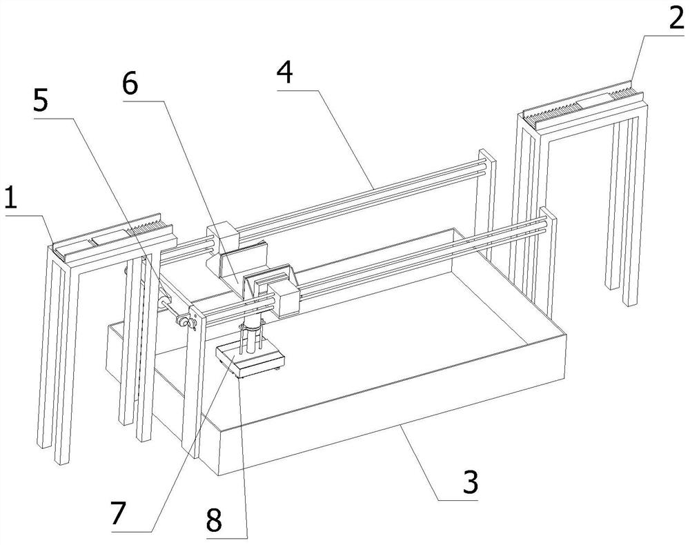
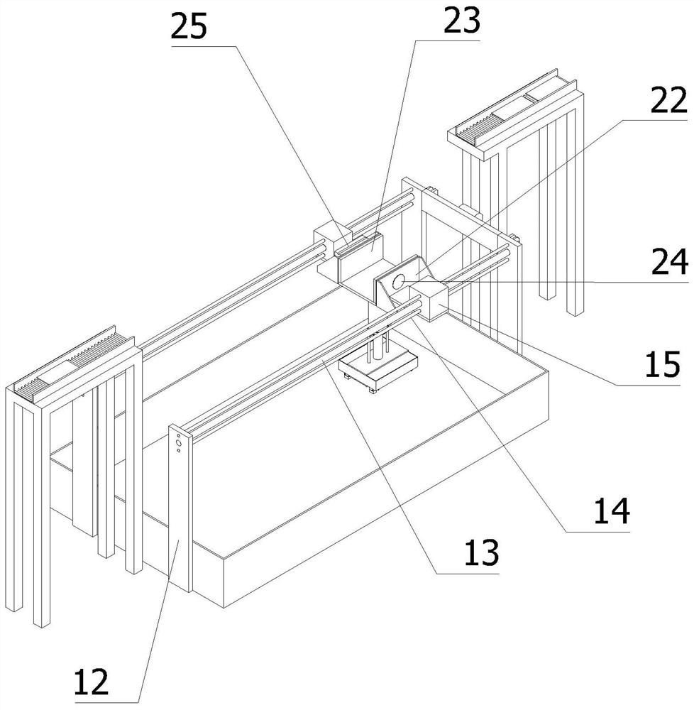
[0063] In order to solve the technical problem of how to etch the circuit board completely and uniformly, such as figure 1 , figure 2 , image 3 , Figure 4 and Figure 8 As shown, the following technical solutions are provided:

[0064] A printed circuit board etching device, comprising:

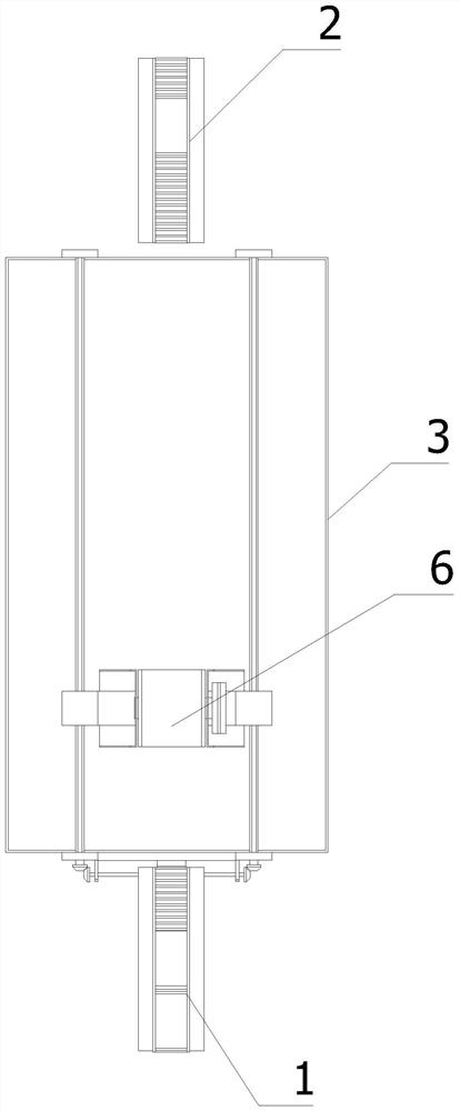
[0065] The feeding conveyor 1 is used to carry out the feeding process of the circuit board to be etched;

[0066] The unloading conveyor 2 is used for unloading the etched circuit board;

[0067] Etching box 3, in order to etch the circuit board to be etched;

[0068] The positioning and turning conveying mechanism is used for positioning, turning over and conveying the circuit board to be etched transported by ...


PUM


Abstract

The invention relates to the technical field of circuit board processing, in particular to a printed circuit board etching device which comprises a feeding conveyor; a discharging conveyor; an etching box; and a positioning, overturning and conveying mechanism. The positioning, overturning and conveying mechanism comprises two groups of translation assemblies arranged on the two sides above the etching box, a synchronous assembly is arranged between the two translation assemblies, an overturning frame is arranged between the two translation assemblies, the two sides of the overturning frame are in transmission connection with the working end of each translation assembly, and a lifting plate is arranged at the bottom of the overturning frame; and two clamping parts are arranged at the top of the lifting plate, each clamping part comprises a [-shaped frame, first synchronous wheels are arranged on the two sides of the interior of each [-shaped frame, and a plurality of protruding parts are arranged on the exterior of each synchronous belt. A circuit board is driven to translate repeatedly through the protruding parts arranged on the two first synchronous belts, so that the circuit board is fully etched during etching, and the etching precision and integrity of the circuit board are improved.

Description

technical field [0001] The invention relates to the technical field of circuit board processing, in particular to a printed circuit board etching device. Background technique [0002] Printed circuit boards are extremely important components in electronic equipment. In order to better process the surface of the circuit board, the circuit board needs to go through many processes in the manufacturing process before the finished product can be prepared. Among them, the etching process of the circuit board is one of the most critical processes in the whole manufacturing process of the circuit board. line. [0003] When an existing etching machine etches a circuit board, the circuit board is clamped by a clamp and immersed in an etching solution, so that the etching solution etches the circuit board. During the etching process, the clamped part of the circuit board is blocked by the fixture, and the etching solution cannot etch the part, and the circuit board cannot be complet...

Claims


Application Information

Patent Timeline
Patent Type & Authority Applications(China)
IPC IPC(8): H05K3/02H05K3/06
CPCH05K3/02H05K3/068
Inventor 李杰王英娟王嘉璐
Owner 山西汇诚晋海科技有限公司
Why Eureka
Try Eureka