
FPGA logic test method and device

A logic testing and logic technology, applied in the field of integrated circuits, can solve problems such as limited signal sampling depth, and achieve the effect of increasing sampling depth and reducing costs

Active Publication Date: 2021-10-15
中航机载系统共性技术有限公司
View PDF3 Cites 0 Cited by
  • Summary
  • Abstract
  • Description
  • Claims
  • Application Information

AI Technical Summary

Problems solved by technology

[0005] Aiming at the defects in the prior art, the present invention provides a FPGA logic test method and device, electronic equipment and medium, to solve the problem that the signal sampling depth is limited when using an embedded logic analyzer for FPGA logic test

Method used


Image

  • FPGA logic test method and device
  • FPGA logic test method and device
  • FPGA logic test method and device

Examples


Embodiment Construction

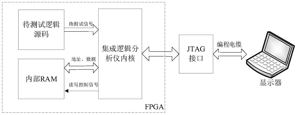
[0065] Embodiments of the technical solutions of the present invention will be described in detail below in conjunction with the accompanying drawings. The following examples are only used to illustrate the technical solution of the present invention more clearly, so they are only examples, and should not be used to limit the protection scope of the present invention.

[0066] It should be noted that, unless otherwise specified, the technical terms or scientific terms used in this application shall have the usual meanings understood by those skilled in the art to which the present invention belongs.

[0067] When using an embedded logic analyzer to perform logic tests on FPGA, it often occurs that the data volume of the logic source code to be tested is greater than the internal storage space and does not match, resulting in low sampling depth. When encountering this kind of problem, an external memory is often used to store the logic source code to be tested. This will bring...


PUM


Abstract

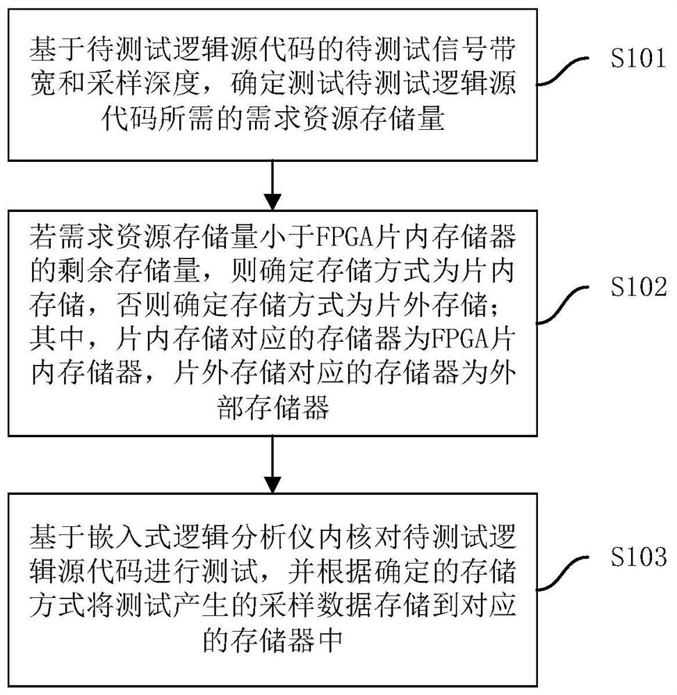
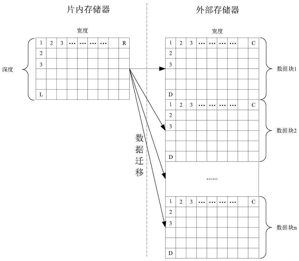
The invention belongs to the technical field of integrated circuits, and particularly provides an FPGA logic test method and device. The method comprises the following steps: based on a to-be-tested signal bandwidth and a sampling depth of a to-be-tested logic source code, determining a required resource storage amount required for testing the to-be-tested logic source code; if the required resource storage amount is smaller than the residual storage amount of the FPGA on-chip memory, determining that the storage mode is on-chip storage, otherwise, determining that the storage mode is off-chip storage, wherein the memory corresponding to the on-chip memory is an FPGA on-chip memory, and the memory corresponding to the off-chip memory is an external memory; and testing the to-be-tested logic source code based on the kernel of the embedded logic analyzer, and storing sampling data generated by the test into a corresponding memory according to the determined storage mode. According to the invention, the problem of low sampling depth caused by an internal storage space during FPGA testing can be avoided, so that the sampling depth during testing is effectively improved.

Description

technical field [0001] The invention relates to the technical field of integrated circuits, in particular to an FPGA logic testing method and device. Background technique [0002] FPGA (Field Programmable Gate Array, Field Programmable Gate Array) is a general-purpose device that includes a large number of repetitive basic units such as programmable logic blocks (CLBs), input-output units (IOBs), and programmable interconnects (PIs). It is especially suitable for the development of new integrated circuits and the production of small batches of ASIC circuits. With its rapid development, it has been widely used in many fields. With the wide application of FPGA, the requirements for its accuracy are getting higher and higher, so all FPGAs need to be tested and verified reasonably. [0003] Currently, there are usually two methods for FPGA logic testing: one is to use an external oscilloscope or logic analyzer, and the other is to use an embedded logic analyzer. Using an exter...

Claims


Application Information

Patent Timeline
IPC IPC(8): G06F11/36G06F3/06G01R31/3177
CPCG06F11/3688G06F11/3664G06F3/0604G06F3/0631G06F3/0638G01R31/3177Y02D10/00
Inventor 贺莹田莉蓉王闯
Owner 中航机载系统共性技术有限公司
Learn More