Array substrate, display panel and preparation method of array substrate

A technology of array substrates and substrate substrates, which is applied in semiconductor/solid-state device manufacturing, electrical components, transistors, etc., can solve problems such as unstable performance, and achieve the effects of improving work stability, avoiding leakage current, and good shading effect

Active Publication Date: 2021-10-22
HKC CORP LTD
View PDF5 Cites 1 Cited by
  • Summary
  • Abstract
  • Description
  • Claims
  • Application Information

AI Technical Summary

Problems solved by technology

[0004] The purpose of this application is to provide an array substrate, a display panel and a method for preparing the array substrate, aiming to solve the problem of unstable performance of the active layer of the thin film transistor of the existing array substrate due to light exposure

Method used


Image

  • Array substrate, display panel and preparation method of array substrate
  • Array substrate, display panel and preparation method of array substrate
  • Array substrate, display panel and preparation method of array substrate

Examples


Embodiment Construction

[0049]It should be understood that the terminology and specific structural and functional details disclosed herein are representative only for describing specific embodiments, but the application can be embodied in many alternative forms and should not be construed as merely Be limited by the examples set forth herein.

[0050] The present application will be described in detail below with reference to the accompanying drawings and optional embodiments.

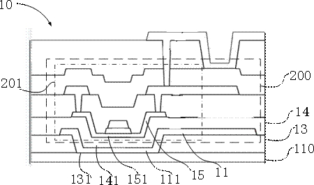
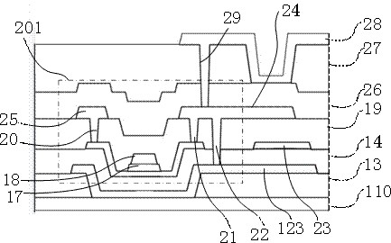
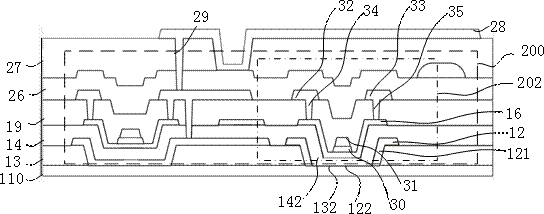
[0051] The present application discloses an array substrate, including a base substrate and a thin film transistor layer, the thin film transistor layer is arranged on the base substrate; the thin film transistor layer includes an active layer; the array substrate also includes a shielding layer , the shielding layer is disposed between the base substrate and the thin film transistor layer, the shielding layer is provided with a groove, and the active layer at least partially protrudes into the groove. Wherein, the orthograp...


PUM


Abstract

The invention discloses an array substrate, a display panel and a preparation method of the array substrate. The array substrate comprises: a substrate body and a film transistor layer, wherein the film transistor layer is arranged on the substrate body, and comprises an active layer; and a shielding layer, wherein the shielding layer is arranged between the substrate body and the film transistor layer, a groove is formed in the shielding layer, and at least part of the active layer extends into the groove. Through the mode, the problem of current leakage caused by illumination of the active layer is improved, and the working stability of the film transistor is improved.

Description

technical field [0001] The present application relates to the field of display technology, and in particular to an array substrate, a display panel and a method for preparing the array substrate. Background technique [0002] Currently, a liquid crystal display panel (Liquid Crystal Display, LCD) and an organic light emitting diode display panel (Organic Light Emitting Diode, OLED) both have an array substrate, and a thin film transistor (Thin Film Transistor, TFT) is disposed on the array substrate. [0003] In thin film transistors, the active layer is a very important film layer, which determines the performance of thin film transistors to a large extent, and many active layers have the problem of leakage current when exposed to light, which will lead to the failure of thin film transistors. Instable performance; in order to solve this technical problem in the prior art, a shielding layer is provided under the active layer, but the effect of the shielding layer is limited...

Claims


Application Information

Patent Timeline
Patent Type & Authority Applications(China)
IPC IPC(8): H01L27/12H01L29/786H01L21/77
CPCH01L27/1222H01L27/1225H01L29/78633H01L29/7869H01L27/1259
Inventor 金璐袁海江
Owner HKC CORP LTD
Why Eureka
Try Eureka