Method for measuring resistance value of circuit board inner layer buried resistor pattern
A circuit board, resistance value technology, applied in the direction of measuring resistance/reactance/impedance, measuring electricity, measuring electrical variables, etc., can solve the problems of resistance value change, loss increase, failure to detect resistance value, etc., to reduce losses and save cost, avoid the effect of scrapping together
- Summary
- Abstract
- Description
- Claims
- Application Information
AI Technical Summary
Problems solved by technology
Method used
Image
Examples
Embodiment 1
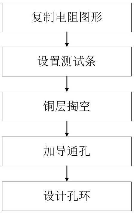
[0041] S1. Copy the buried resistance pattern in the unit to the edge of the board to form a buried resistance pattern on the side of the board; set the buried resistance pattern on the side of the board according to the resistance value of the buried resistance, the width of the buried resistance pattern on the side of the board remains unchanged, and the length is set according to the preset ratio;
[0042] S2. Set copper wires and test patterns at both ends of the embedded resistance pattern on the edge of the board to form a test strip; the copper wires are arranged at both ends of the embedded resistance pattern on the edge of the board, and the test pattern is arranged at both ends of the copper wire;
[0043] S3. Empty the surface copper at the position of the test strip on the edge of the board to be hollowed out at other levels; expose the test strip;
[0044] S4. Drill through holes at the position of the test pattern on the board and metallize the holes;
[0045] S5...
Embodiment 2
[0049] S1. Copy the buried resistance pattern in the unit to the edge of the board to form a buried resistance pattern on the side of the board; set the buried resistance pattern on the side of the board according to the resistance value of the buried resistance, the width of the buried resistance pattern on the side of the board remains unchanged, and the length is set according to the preset ratio;
[0050] S2. Set copper wires and test patterns at both ends of the embedded resistance pattern on the edge of the board to form a test strip; the copper wires are arranged at both ends of the embedded resistance pattern on the edge of the board, and the test pattern is arranged at both ends of the copper wire;
[0051] S3. Empty the surface copper at the position of the test strip on the edge of the board to be hollowed out at other levels; expose the test strip;
[0052] S4. Drill through holes at the position of the test pattern on the board and metallize the holes;
[0053] S5...
PUM
 Abstract
Description
Claims
Application Information
 - R&D
- Intellectual Property
- Life Sciences
- Materials
- Tech Scout
- Unparalleled Data Quality
- Higher Quality Content
- 60% Fewer Hallucinations
Browse by: Latest US Patents, China's latest patents, Technical Efficacy Thesaurus, Application Domain, Technology Topic, Popular Technical Reports.
© 2025 PatSnap. All rights reserved.Legal|Privacy policy|Modern Slavery Act Transparency Statement|Sitemap|About US| Contact US: help@patsnap.com

