Packaging structure formed by stacking multiple interconnected flip chips and preparation method thereof

A technology of flip-chip and packaging structure, which is applied in semiconductor/solid-state device manufacturing, electrical components, electric solid-state devices, etc. It can solve the problems of large packaging structure area and inability to stack, and achieve miniaturization, size reduction, and reduction Effect of Area Utilization

Pending Publication Date: 2021-10-26
VERISILICON MICROELECTRONICS NANJING CO LTD +2
View PDF0 Cites 0 Cited by
  • Summary
  • Abstract
  • Description
  • Claims
  • Application Information

AI Technical Summary

Problems solved by technology

[0005] In view of the above-mentioned shortcomings of the prior art, the object of the present invention is to provide a packaging structure of multiple interconnected flip-chip stacks and its preparation method, which is used to solve the problem of the packaging process of flip-chip chips in the prior art. Among them, because they must be placed side by side, they cannot be stacked, resulting in problems such as a larger package structure

Method used


Image

  • Packaging structure formed by stacking multiple interconnected flip chips and preparation method thereof
  • Packaging structure formed by stacking multiple interconnected flip chips and preparation method thereof
  • Packaging structure formed by stacking multiple interconnected flip chips and preparation method thereof

Examples


Embodiment 1

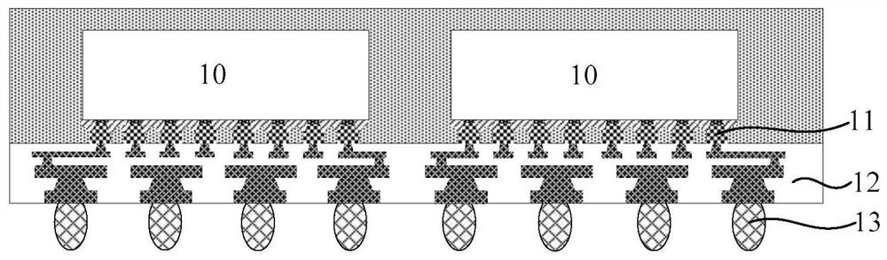
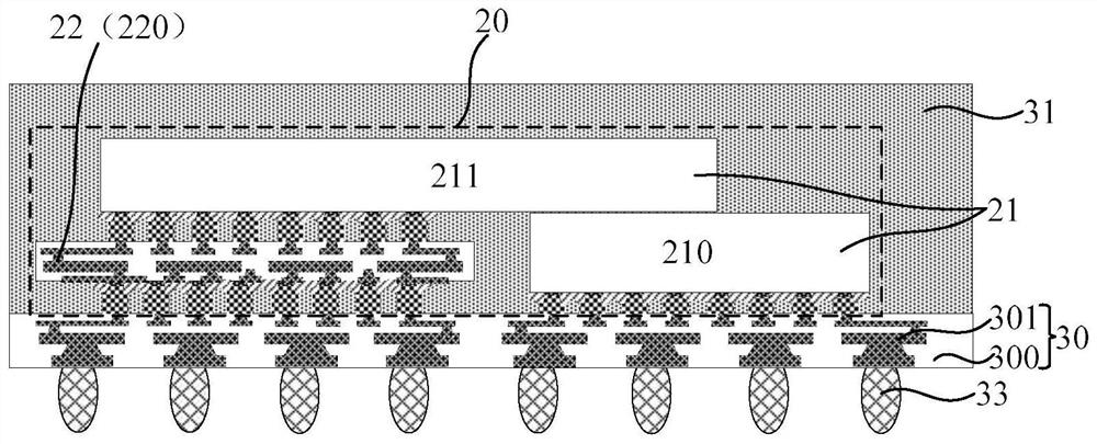
[0058] Such as Figure 2 to Figure 5 As shown, this embodiment provides a package structure of multiple interconnected flip-chip stacks, the package structure comprising:

[0059] The rewiring layer 30 is arranged on the bottom layer;

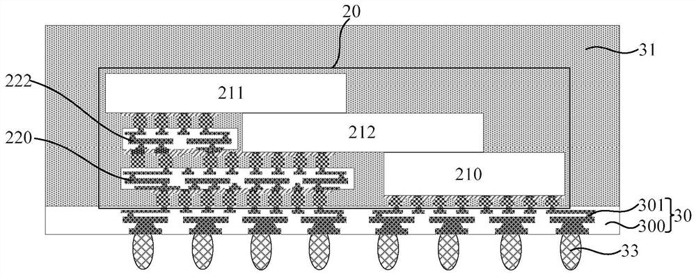
[0060] The flip chip stacking structure 20 is stacked on the upper surface of the rewiring layer 30 along the vertical direction; the flip chip stacking structure 20 includes N layers of flip chips 21 and N-1 layers of interposers 22, N≥2 ; Wherein, the first layer flip chip 210 and the first layer adapter board 220 are welded on the rewiring layer 30, the Mth layer adapter board 221 is welded on the M-1 layer adapter board 222, the Mth layer The layer flip chip 211 is stacked on the M-1 layer flip chip 212 and the M-1 layer adapter plate 222, and is non-electrically connected with the M-1 layer flip chip 212, Electrically connected to the M-1th layer adapter board 222, N≥M≥2;

[0061] The encapsulation layer 31 covers the flip chip stack st...

Embodiment 2

[0071] Such as Figure 6 to Figure 13 As shown, this embodiment provides a method for preparing a package structure of interconnected multiple flip-chip stacks, and the package structure of interconnected multiple flip-chip stacks described in the first embodiment can be manufactured by this preparation method. However, it is not limited thereto. For the beneficial effects it can achieve, please refer to Embodiment 1, which will not be repeated here.

[0072] Specifically, such as Image 6 Shown, described preparation method comprises the following steps:

[0073] S1, preparing the rewiring layer and the adapter board;

[0074] S2, stacking a flip-chip stacking structure vertically on the upper surface of the rewiring layer, the flip-chip stacking structure includes N layers of flip chips and N-1 layers of interposer boards, N≥2, including: The first layer of flip chip and the first layer of the adapter board are welded on the rewiring layer; the Mth layer of the adapter bo...


PUM


Abstract

The invention provides a packaging structure formed by stacking a plurality of interconnected flip chips and a preparation method of the packaging structure. The packaging structure comprises a rewiring layer; a flip chip stacking structure stacked on the upper surface of the rewiring layer in the vertical direction, wherein the flip chip stacking structure comprises N layers of flip chips and N-1 layers of adapter plates, and N is greater than or equal to 2, the first layer of flip chip and the first layer of adapter plate are welded on the rewiring layer, the Mth layer of adapter plate is welded on the (M-1) th layer of adapter plate, the Mth layer of flip chip is stacked on the (M-1) th layer of flip chip and the (M-1) th layer of adapter plate, is in non-electrical connection with the (M-1) th layer of flip chip and is electrically connected with the (M-1) th layer of adapter plate, and M is greater than or equal to 2 and greater than or equal to N; and an encapsulation layer. According to the packaging structure, a packaging structure in which the flip chips are packaged in a horizontal arrangement mode in the prior art is changed into a three-dimensional packaging structure in which the flip chips are packaged in a vertical arrangement mode, the area utilization rate of stacked packaging of the multiple flip chips is effectively reduced, the size of a packaging body is reduced, and miniaturization of products is facilitated.

Description

technical field [0001] The invention belongs to the technical field of semiconductor packaging, and in particular relates to a packaging structure of multiple interconnected flip-chip stacks and a preparation method thereof. Background technique [0002] With the trend of multi-function, high performance and miniaturization of electronic products, high-density microelectronic assembly technology has gradually become the mainstream in the new generation of electronic products. In order to cope with the development of the new generation of electronic products, especially the development of smart phones, PDAs, ultrabooks and other products, the size of the chip is developing in the direction of higher density, faster speed, smaller size and lower cost. The packaging of integrated circuits has also been proposed to develop in the direction of light, thin, small and high performance, and the packaging is required to be able to perform high-density interconnection, and to be able ...

Claims


Application Information

Patent Timeline
IPC IPC(8): H01L25/16H01L23/31H01L23/488H01L21/60H01L21/56
CPCH01L25/16H01L23/3128H01L24/02H01L24/13H01L24/11H01L21/56H01L2224/02331H01L2224/02333H01L2224/02381H01L2224/02373H01L2224/111H01L2224/13008
Inventor 郑清毅陈银龙
Owner VERISILICON MICROELECTRONICS NANJING CO LTD
Why Eureka
Try Eureka