Light-emitting assembly, manufacturing method thereof and light-emitting device

A technology of light-emitting components and manufacturing methods, which is applied in the direction of electrical components, electric solid-state devices, semiconductor devices, etc., can solve the problems of separation and falling off of light-emitting components, color deviation, mixed light, etc., to improve push-pull resistance performance, improve display quality, The effect of increasing the contact area

Pending Publication Date: 2021-10-29
SHENZHEN CHINA STAR OPTOELECTRONICS TECH CO LTD
View PDF0 Cites 2 Cited by
  • Summary
  • Abstract
  • Description
  • Claims
  • Application Information

AI Technical Summary

Problems solved by technology

The direction of light transmission is in figure 1 Indicated by arrows, since the distribution area of ​​the light-emitting components 92 is small, if the light colors emitted by two adjacent light-emitting components 92 are different, light mixing will occur at the intersecting light positions, resulting in color deviation
Moreover, because the contact area between the bottom of the anode pad 922 and the bottom of the cathode pad 923 and the pad 94 on the substrate 91 is small, the light-emitting component 92 will be separated from the substrate 91 when pushed and pulled by an external force.

Method used


Image

  • Light-emitting assembly, manufacturing method thereof and light-emitting device
  • Light-emitting assembly, manufacturing method thereof and light-emitting device
  • Light-emitting assembly, manufacturing method thereof and light-emitting device

Examples


Embodiment 1

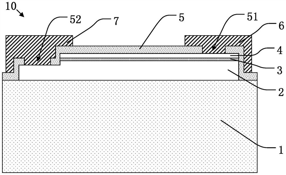
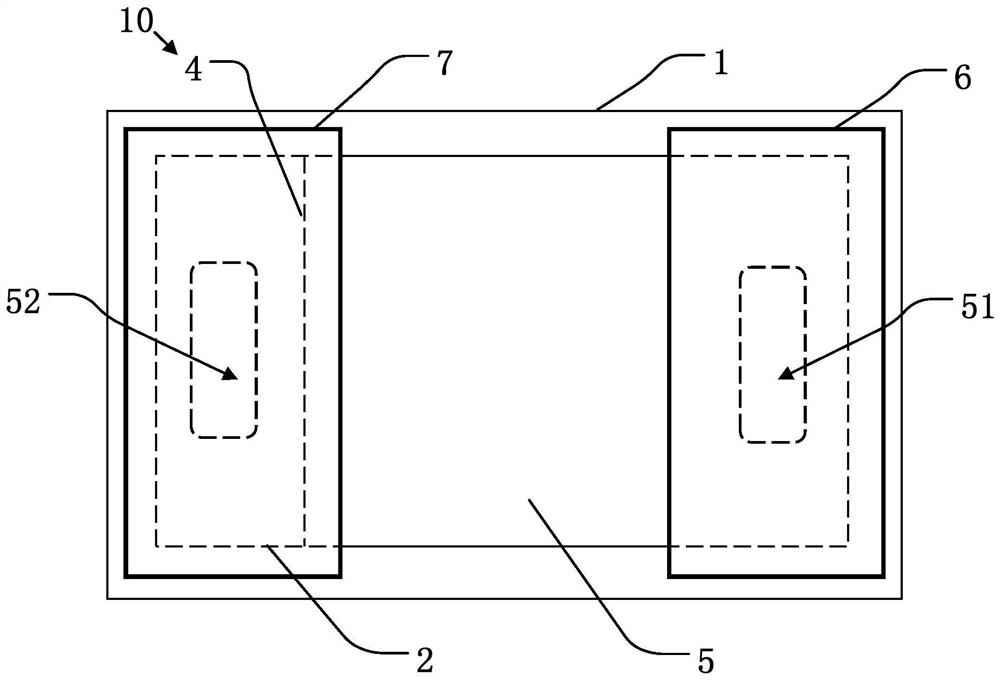
[0051] see figure 2 , image 3 , Embodiment 1 of the present application provides a light-emitting component 10 . figure 2 It is a cross-sectional view of the light-emitting component 10 provided in Embodiment 1 of the present application; image 3 It is a top view of the light-emitting component 10 provided in Embodiment 1 of the present application. The light-emitting component 10 includes an epitaxial substrate 1, an N-type material layer 2 disposed on the epitaxial substrate 1, a light-emitting layer 3 disposed on the N-type material layer 2, and a light-emitting layer 3 disposed on the light-emitting layer 3. The P-type material layer 4, the passivation layer 5 covering the P-type material layer 4, the light-emitting layer 3 and the N-type material layer 2, and the anode pad 6 arranged on the passivation layer 5 and the cathode pad 7; specifically, the passivation layer 5 is provided with a first via hole 51 on the P-type material layer 4, and the passivation layer 5...

Embodiment 2

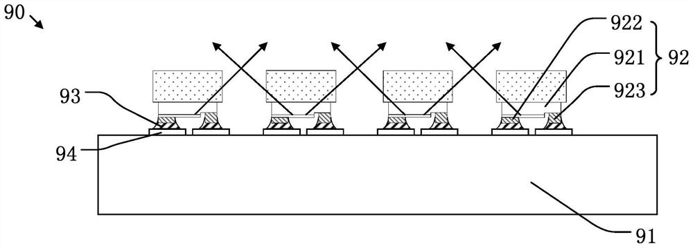
[0071] see Figure 6 , Figure 7, Embodiment 2 of the present application provides a light-emitting component 10a, including all the technical features of Embodiment 1, the difference is that the light-emitting component 10a in Embodiment 2 is further on the upper surface of the epitaxial substrate 1, along The epitaxial substrate 1 is surrounded by auxiliary grooves 11 , and the anode pad 6 and the cathode pad 7 extend into the auxiliary groove 11 . This can further make the anode pad 6 and the cathode pad 7 cover the surrounding surface of the epitaxial substrate 1, thereby increasing the coverage of the anode pad 6 and the cathode pad 7 on the light-emitting surface. layer 3, so as to further improve the chance of light being reflected to the epitaxial substrate 1 between the anode pad 6 and the cathode pad 7, and avoid the side-emitted light from adjacent two light-emitting components Mixed light appears between 10a.

[0072] Similarly, see Figure 7 , the anode pad 6 ...

Embodiment 3

[0078] see Figure 10 , Figure 11 , Embodiment 3 of the present application provides a light-emitting assembly 10b, including all the technical features of Embodiment 2, the difference is that the light-emitting assembly 10 in Embodiment 3 is further provided with a cutting recess in the auxiliary groove 11 The groove 12 , the anode pad 6 and the cathode pad 7 extend into the cutting groove 12 . This can further make the anode pad 6 and the cathode pad 7 cover the surrounding surface of the epitaxial substrate 1 and fill in the auxiliary groove 11 and the cutting groove 12, thereby increasing the The anode pad 6 and the cathode pad 7 are covered in the range of the light-emitting component 10b, thereby further increasing the chance of laterally emitted light being reflected between the anode pad 6 and the cathode pad 7 , avoid light mixing between two adjacent light-emitting components 10 .

[0079] Similarly, the anode pad 6 partially covers the three sides of the passiva...


PUM


Abstract

The invention discloses a light-emitting assembly, a manufacturing method thereof and a light-emitting device. The light-emitting assembly comprises an epitaxial substrate, an N-type material layer, a light-emitting layer, a P-type material layer, a passivation layer, an anode bonding pad and a cathode bonding pad, wherein the anode bonding pad extends from the upper surface of the P-type material layer to the upper surface of the epitaxial substrate along the passivation layer; and the cathode bonding pad extends from the upper surface of the P-type material layer to the surface of the N-type material along the passivation layer and then extends to the upper surface of the epitaxial substrate. On the one hand, the bonding pads are arranged on the side wall and the bottom of the light-emitting layer to form the light-emitting assemblies, color deviation caused by light mixing of different-color light rays emitted by the two adjacent light-emitting assemblies is avoided, and therefore the display quality is improved; on the other hand, the solder paste is coated on the side wall and the bottom of the bonding pad to form the solder paste layer, so that the contact area of the solder paste layer and the bonding pad of the driving substrate is increased, the push-pull resistance of the light-emitting assembly is improved, the light-emitting assembly is prevented from falling off due to stress, and the display quality is improved.

Description

technical field [0001] The invention relates to the field of display technology, in particular to a light-emitting component, a manufacturing method and a light-emitting device. Background technique [0002] As the high-end TV market has higher and higher requirements for picture quality, improving display picture quality has become a new demand for high-end TVs. Currently limited by technologies such as compensation circuits, backplane technology, and driver design, the application of 8K organic light-emitting diodes (OLEDs) has yet to be developed. As a new display technology, submillimeter light-emitting diodes (Mini LEDs) have advantages over organic light-emitting diodes and dual-LCD displays in terms of brightness and power consumption. [0003] However, as the light-emitting diode chips of submillimeter light-emitting diodes (Mini LEDs) and micro-light-emitting diodes (Micro-LEDs) become smaller and smaller, the pad area becomes smaller and smaller correspondingly, r...

Claims


Application Information

Patent Timeline
Patent Type & Authority Applications(China)
IPC IPC(8): H01L27/15H01L33/36
CPCH01L27/156H01L33/36
Inventor 胡道兵
Owner SHENZHEN CHINA STAR OPTOELECTRONICS TECH CO LTD
Why Eureka
Try Eureka