Sensing element substrate and display device including same

A technology for sensing components and display devices, applied in electrical components, radiation control devices, electric solid state devices, etc., can solve the problems of reducing the contrast quality of fingerprint images, insufficient light/dark current ratio, affecting the contrast quality of fingerprint images, etc. The effect of improving contrast quality, improving light/dark current ratio, and good circuit coupling efficiency

Active Publication Date: 2021-11-02
AU OPTRONICS CORP
View PDF5 Cites 0 Cited by
  • Summary
  • Abstract
  • Description
  • Claims
  • Application Information

AI Technical Summary

Problems solved by technology

However, the optical collimation design needs to limit the light-receiving area of ​​the sensing element, resulting in a decrease in the photocurrent (Iph), resulting in a similar light / dark current value, that is, an insufficient light / dark current ratio, which in turn affects the fingerprint image contrast quality
If the non-illuminated area of ​​the sensing element is reduced to reduce the dark current, the capacitance of the sensing element will decrease, resulting in poor circuit coupling efficiency under the action of the active photosensitive circuit, resulting in low output voltage of the fingerprint and compression of the peak of the fingerprint / Grain and valley contrast, which will also reduce the contrast quality of the fingerprint image

Method used


Image

  • Sensing element substrate and display device including same
  • Sensing element substrate and display device including same
  • Sensing element substrate and display device including same

Examples


Embodiment Construction

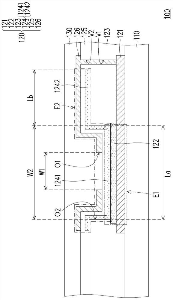
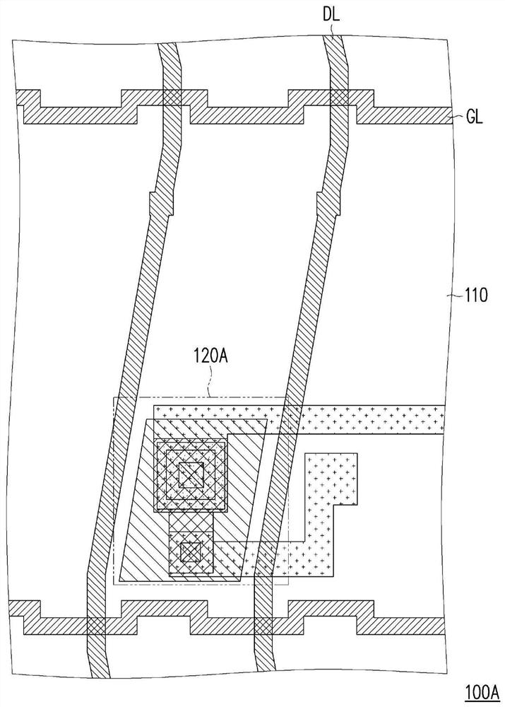
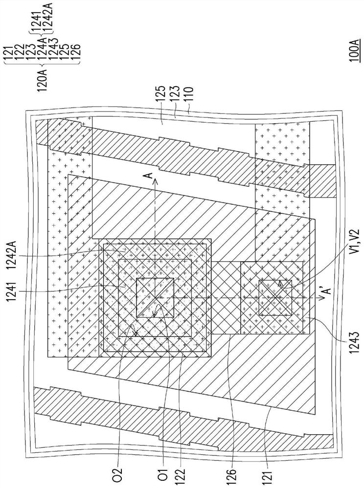
[0104] figure 1 is a schematic cross-sectional view of a sensing element substrate 100 according to an embodiment of the present invention. Please refer to figure 1 The sensing element substrate 100 includes a substrate 110 and a sensing element 120 , and the sensing element 120 is located on the substrate 110 . The sensing element 120 includes a first electrode 121 , a sensing layer 122 , a second electrode 124 , a first insulating layer 125 and a conductive layer 126 . The first electrode 121 is located on the substrate 110 . The second electrode 124 overlaps the first electrode 121 . The sensing layer 122 is located between the second electrode 124 and the first electrode 121 . The conductive layer 126 overlaps the second electrode 124 and is electrically connected to the first electrode 121 , wherein the conductive layer 126 has a first opening O1 , and the first opening O1 overlaps the sensing layer 122 . The first insulating layer 125 is located between the conducti...


PUM


Abstract

The invention provides a sensing element substrate and a display device comprising the same. The sensing element substrate includes a substrate and a sensing element. The sensing element is located on the substrate and comprises a first electrode, a second electrode, a sensing layer, a conductive layer and a first insulating layer. The first electrode is located on the substrate. The second electrode overlaps the first electrode. The sensing layer is located between the second electrode and the first electrode. The conductive layer overlaps the second electrode and is electrically connected to the first electrode. The conductive layer has a first opening which overlaps the sensing layer. The first insulating layer is located between the conductive layer and the second electrode.

Description

technical field [0001] The present invention relates to a sensing element substrate, in particular to a display device including the sensing element substrate. Background technique [0002] The development of display devices is changing with each passing day, especially the full-screen design has become the mainstream of small and medium-sized screen specifications. In order to achieve a full screen, the fingerprint recognition function is integrated into the screen display iFP (in-cell Fingerprint Sensing) is its key technology, and the full-screen non-fixed-point fingerprint recognition function is expected to support a variety of applications, improving user experience and Increase the added value of the panel, for the current key development projects. [0003] In terms of practical application requirements, iFP needs to be equipped with a light collimation design to overcome the interference of reflected light from adjacent peaks / valleys of fingerprints caused by the th...

Claims


Application Information

Patent Timeline
Patent Type & Authority Applications(China)
IPC IPC(8): G06K9/00
CPCH01L27/146H01L27/14678G06V40/1306H01L27/1255
Inventor 陈铭耀罗睿骐黄伟明
Owner AU OPTRONICS CORP
Why Eureka
Try Eureka