MEMS sensor and preparation method thereof

A sensor and electrode layer technology, applied in the field of MEMS sensor and its preparation, can solve the problems of complex preparation process, large temperature drift, low reliability, etc., and achieve the effects of simplifying the preparation process, improving detection accuracy and reducing temperature drift

Pending Publication Date: 2021-11-05
HANGZHOU SILAN MICROELECTRONICS
View PDF10 Cites 0 Cited by
  • Summary
  • Abstract
  • Description
  • Claims
  • Application Information

AI Technical Summary

Problems solved by technology

[0004] The purpose of the present invention is to provide a MEMS sensor and its preparation method to solve the problems of complex preparation process, large temperature drift and low reliability of the existing MEMS sensor.

Method used


Image

  • MEMS sensor and preparation method thereof
  • MEMS sensor and preparation method thereof
  • MEMS sensor and preparation method thereof

Examples


Embodiment 1

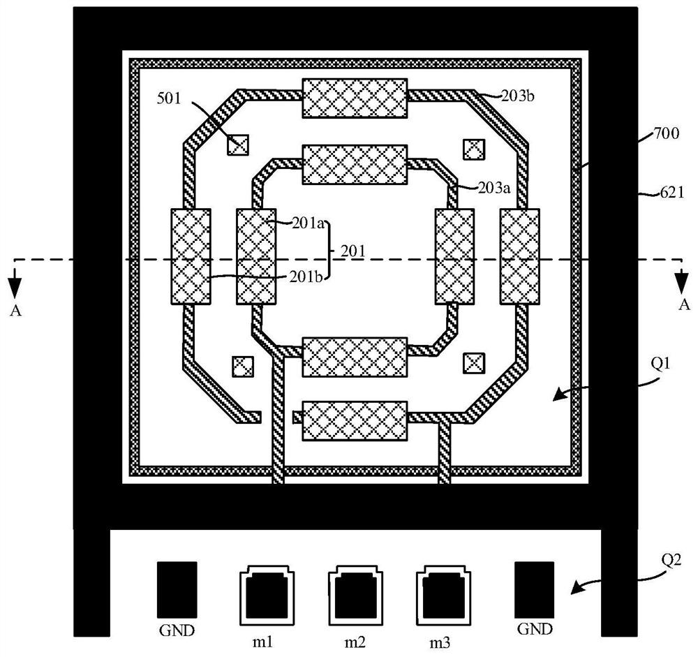
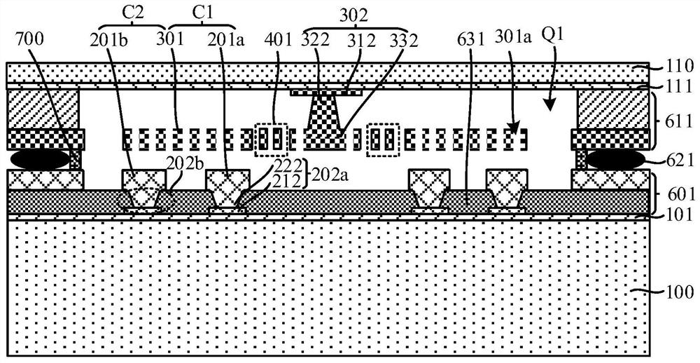
[0070] Figure 1a A schematic plan view of the first substrate provided in this embodiment, Figure 1b A schematic plan view of the second substrate provided in this embodiment, figure 2 A schematic cross-sectional view of the MEMS sensor along the direction AA is provided for this embodiment. In this embodiment, the MEMS sensor is a force sensor. Such as Figure 1a , Figure 1b and figure 2 As shown, the force sensor includes a first substrate 100, a second substrate 110 and a support structure between the first substrate 100 and the second substrate 110, the first substrate 100 The front side is opposite to the front side of the second substrate 110, and the support structure together with the first substrate 100 and the second substrate 110 forms a closed cavity Q1, wherein the first substrate The bottom 100 and the second substrate 110 serve as upper and lower surfaces of the cavity Q1 respectively, and the support structure serves as a side surface of the cavity.

...

Embodiment 2

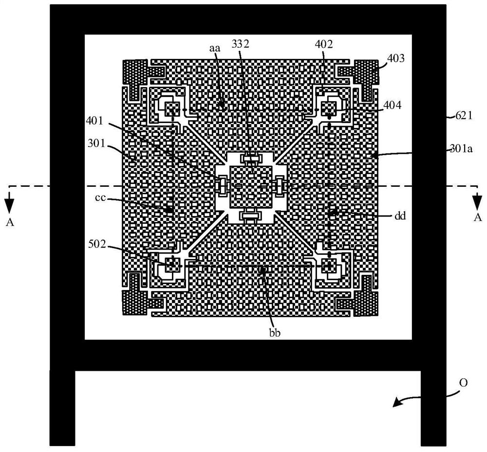
[0129] Figure 4 Schematic diagram of the structure of the first substrate provided in this embodiment, Figure 5 A schematic cross-sectional view of the MEMS sensor along the BB direction is provided for this embodiment. Such as Figure 4 and Figure 5 As shown, in this embodiment, the structure on the second substrate 110 is the same as that in Embodiment 1, and the structure on the first substrate 100 is different from that in Embodiment 1. Specifically, in this embodiment, each The two first conductive connection structures in each of the electrode groups are located in the region between the corresponding two first electrode layers 201, and the two first conductive connection structures are arranged close to each other.

[0130] read on Figure 4 and Figure 5 Taking the first electrode layer 201a and the first electrode layer 201b as an example, the first conductive connection structure 202a and the first conductive connection structure 202b are both located on the ...


PUM


Abstract

According to the MEMS sensor and a preparation method thereof provided by the invention, when the back surface of a second substrate is stressed, second electrode layers deform, and the distances between the two first electrode layers and the corresponding second electrode layers change along opposite directions, the magnitude of the externally applied pressure can be determined by detecting the difference between the capacitance values of the detection capacitors formed by the second electrode layers and the two first electrode layers, and pressure detection is achieved.

Description

technical field [0001] The invention relates to the technical field of micro-microphones, in particular to a MEMS sensor and a preparation method thereof. Background technique [0002] Since the concept of MEMS (Microelectromechanical System, MEMS) device was formed in the 1970s, MEMS device has progressed from the object of laboratory exploration to the object of high-level system integration, and has been widely used in mass consumer devices , exhibiting an astonishing and steady growth. The MEMS device includes a movable MEMS component, and various functions of the MEMS device can be realized by sensing or controlling the motion physical quantity of the movable MEMS component. An example is a force sensor, which can detect whether a pressing action and / or how hard it is pressed, such as a pressure touch button on a mobile phone. [0003] Known force sensors mainly include piezoresistor and capacitive. At present, the manufacturing process of capacitive force sensors is...

Claims


Application Information

Patent Timeline
Patent Type & Authority Applications(China)
IPC IPC(8): B81B7/02B81C1/00
CPCB81B7/02B81C1/00166B81B2201/0257
Inventor 汪建平胡铁刚
Owner HANGZHOU SILAN MICROELECTRONICS
Why Eureka
Try Eureka