LED chip mass transfer method with high stripping yield and convenient film inversion

A technology of LED chip and transfer method, which is applied in semiconductor devices, electrical components, semiconductor/solid-state device manufacturing, etc., and can solve problems such as Mini/Micro LED chip 3' cracking

Active Publication Date: 2021-11-05
HCP TECH CO LTD
View PDF29 Cites 2 Cited by
  • Summary
  • Abstract
  • Description
  • Claims
  • Application Information

AI Technical Summary

Problems solved by technology

Since there is no protection of the adhesive layer 1', it is easy to cause the Mini/Micro LE

Method used


Image

  • LED chip mass transfer method with high stripping yield and convenient film inversion
  • LED chip mass transfer method with high stripping yield and convenient film inversion
  • LED chip mass transfer method with high stripping yield and convenient film inversion

Examples


Embodiment Construction

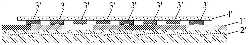
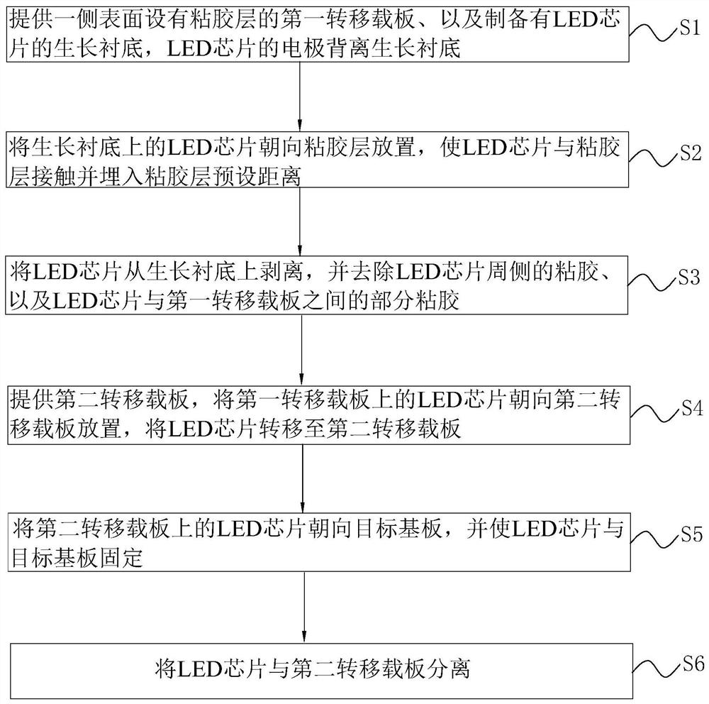
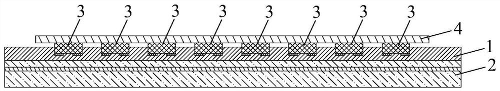
[0024] In order to describe the content, structural features, goals and effects of the present invention in detail, the technical solutions in the embodiments of the present invention will be clearly and completely described below in conjunction with the accompanying drawings in the embodiments of the present invention. Obviously, the described implementation Examples are only some embodiments of the present invention, but not all embodiments. Based on the embodiments of the present invention, all other embodiments obtained by persons of ordinary skill in the art without creative efforts fall within the protection scope of the present invention.

[0025] In the description of the invention, it should be understood that the orientation or positional relationship indicated by the terms "upper", "lower", "horizontal", "vertical" etc. is based on the orientation or positional relationship shown in the drawings, and is only for It is convenient to describe the present invention and...


PUM


Abstract

The invention discloses an LED chip mass transfer method with high stripping yield and convenient film inversion. According to the method, an LED chip is embedded into an adhesive layer of a first transfer support plate in the process of transferring the LED chip from a growth substrate to the first transfer support plate through a laser stripping mode; the LED chip is protected through the adhesive layer, so that the problem that when the LED chip is stripped from the growth substrate, the LED chip is broken is solved, and the transfer yield of the LED chip is improved; and on the basis, after the LED chip is stripped from the growth substrate, subsequent film inversion is carried out, and before the LED chip is transferred from the first transfer carrier plate to a second transfer carrier plate, part of the adhesive at the peripheral side of the LED chip and part of the adhesive between the LED chip and the first transfer carrier plate are removed, and only the rest part of the adhesive is adhered between the LED chip and the first transfer carrier plate, so that the LED chip can be conveniently separated from the first transfer carrier plate in the process of transferring the LED chip from the first transfer carrier plate to the second transfer carrier plate.

Description

technical field [0001] The invention relates to the technical field of LED chip transfer, in particular to a mass transfer method of LED chips with high peeling yield and convenient film flipping. Background technique [0002] After the Mini / Micro LED chips are usually produced, they will be transferred in large quantities. Specifically, a large number (usually tens of thousands to millions) of Mini / Micro LED chips are transferred to the circuit substrate in an accurate and orderly manner to form an LED array. . For some Mini / Micro LED chips whose electrodes are away from the growth substrate, the mass transfer process involves a second inversion process. The mass transfer process of these Mini / Micro LED chips generally includes: using a detachable adhesive layer A first transfer carrier, the Mini / Micro LED chip is transferred from the growth substrate (such as sapphire substrate) to the first transfer carrier by laser lift-off; The Mini / Micro LED chips on the carrier boar...

Claims


Application Information

Patent Timeline
IPC IPC(8): H01L33/48H01L21/683
CPCH01L33/48H01L21/6836H01L2933/0033H01L2221/68368H01L2221/68386
Inventor 薛水源庄文荣孙明付小朝
Owner HCP TECH CO LTD
Why Eureka
Try Eureka