Digital test vector automatic learning method and system

A technology of automatic learning and digital testing, applied in the field of electronics, can solve the problems of complex logic chip vector programming difficulty and low debugging efficiency, so as to save writing time and efficiency, improve development efficiency, and reduce programming difficulty.

Active Publication Date: 2021-11-12
NANJING MACROTEST SEMICON TECH CO LTD
View PDF5 Cites 2 Cited by
  • Summary
  • Abstract
  • Description
  • Claims
  • Application Information

AI Technical Summary

Problems solved by technology

[0005] Purpose of the invention: In order to overcome the deficiencies in the prior art, the present invention provides a method and system for automatically learning digital test vectors. The present invention improves the writing and debugging efficiency of pattern vectors, and solves the difficulty of writing vectors for complex logic chips and the difficulty of debugging. The problem of inefficiency

Method used


Image

  • Digital test vector automatic learning method and system
  • Digital test vector automatic learning method and system
  • Digital test vector automatic learning method and system

Examples


Embodiment Construction

[0035] Below in conjunction with accompanying drawing and specific embodiment, further illustrate the present invention, should be understood that these examples are only for illustrating the present invention and are not intended to limit the scope of the present invention, after having read the present invention, those skilled in the art will understand various aspects of the present invention All modifications of the valence form fall within the scope defined by the appended claims of the present application.

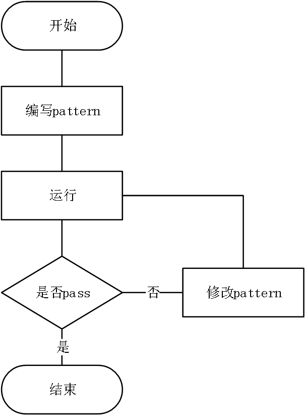
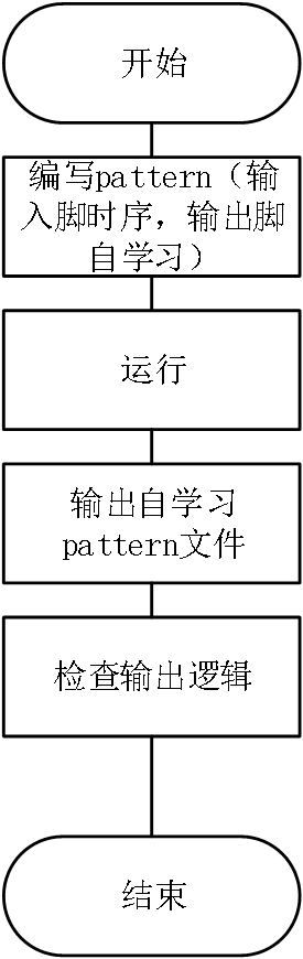
[0036] A method for automatic learning of digital test vectors, such as Figure 2-7 shown, including the following steps:

[0037] Step 1. Write a graphic file. The graphic file includes input pin timing and output pin timing. The input pin timing is given by the device under test, and the input pin timing includes clock timing, driving data timing, and enable signal timing. The timing of the output pin is set to the learning state. When writing the pattern graphic...


PUM


Abstract

The invention discloses a digital test vector automatic learning method and system. The system comprises an upper computer, a pattern generator PG, a driver DRIVER, a comparator COMPARE, and a historical memory HRAM. A pattern file is compiled, the pattern file comprises an input pin time sequence and an output pin time sequence, the input pin time sequence is given by a tested device, and the output pin time sequence is set to be in a learning state; the pattern file is run, and a running state is recorded; the recorded running state data are read, and the output pin state recorded in a certain time in the running state data is obtained; and an output pin time sequence in the running pattern file is corrected according to the obtained output pin state to obtain a corrected output time sequence, and further a corrected pattern file is obtained. The development efficiency is greatly improved, the writing of the characteristics of the chip output pin is reduced, and the compiling difficulty is reduced.

Description

technical field [0001] The invention relates to a method and system for writing and debugging digital vectors, belonging to the technical field of electronics. Background technique [0002] In IC testing, if it is distinguished by function, it can be divided into digital integrated circuits, analog integrated circuits and digital / analog hybrid integrated circuits. Among them, in digital integrated circuit testing, the complexity and task load of test program writing are relatively large, but the writing and debugging of digital vectors account for the most important part. [0003] As the logic functions of the current chip are becoming more and more complex, more and more test cases need to be written. Not only the logic of the driving pin of the device under test needs to be written, but also the corresponding output logic needs to be written. When faced with the situation of new product features to be verified, the function verification of the chip output pin is more comp...

Claims


Application Information

Patent Timeline
Patent Type & Authority Applications(China)
IPC IPC(8): G06F11/22
CPCG06F11/2221G06F11/2273
Inventor 刘万超毛国梁
Owner NANJING MACROTEST SEMICON TECH CO LTD
Why Eureka
Try Eureka