Flexible circuit board, manufacturing method thereof and display device

A flexible circuit board, flexible circuit board technology, applied in the direction of printed circuit manufacturing, printed circuit, printed circuit components, etc., can solve the problems of low yield rate of flexible circuit board process, solder joints, loss of flexible circuit board, etc., to achieve The effect of improving welding quality and welding yield

Pending Publication Date: 2021-11-12
BOE TECH GRP CO LTD +1
View PDF10 Cites 0 Cited by
  • Summary
  • Abstract
  • Description
  • Claims
  • Application Information

AI Technical Summary

Problems solved by technology

[0005] The flexible circuit board with the stacked structure of the multi-layer board in the existing process is prone to bubbles and defects such as welding defects during welding, resulting in a low yield rate of the flexible circuit board process, and there are flexible circuit boards that have not been detected due to defective bonding and flow into the terminal the risk of greater loss

Method used


Image

  • Flexible circuit board, manufacturing method thereof and display device
  • Flexible circuit board, manufacturing method thereof and display device
  • Flexible circuit board, manufacturing method thereof and display device

Examples


Embodiment Construction

[0044] In order to make the purpose, technical solutions and advantages of the embodiments of the present disclosure clearer, the technical solutions of the embodiments of the present disclosure will be clearly and completely described below in conjunction with the accompanying drawings of the embodiments of the present disclosure. Apparently, the described embodiments are some of the embodiments of the present disclosure, not all of them. Based on the described embodiments of the present disclosure, all other embodiments obtained by persons of ordinary skill in the art without creative effort fall within the protection scope of the present disclosure.

[0045] Unless otherwise defined, the technical terms or scientific terms used in the present disclosure shall have the usual meanings understood by those skilled in the art to which the present disclosure belongs. "First", "second" and similar words used in the present disclosure do not indicate any order, quantity or importan...


PUM

PropertyMeasurementUnit
Melting pointaaaaaaaaaa

Abstract

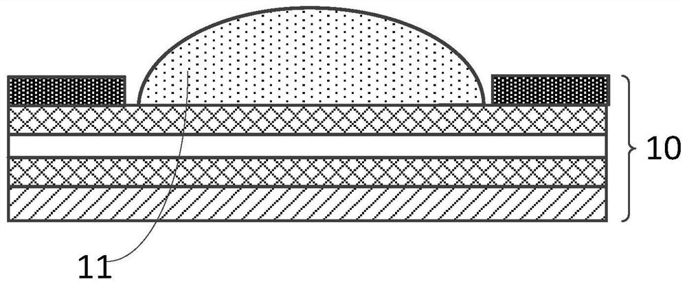
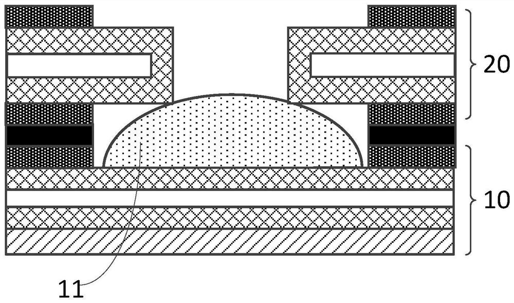
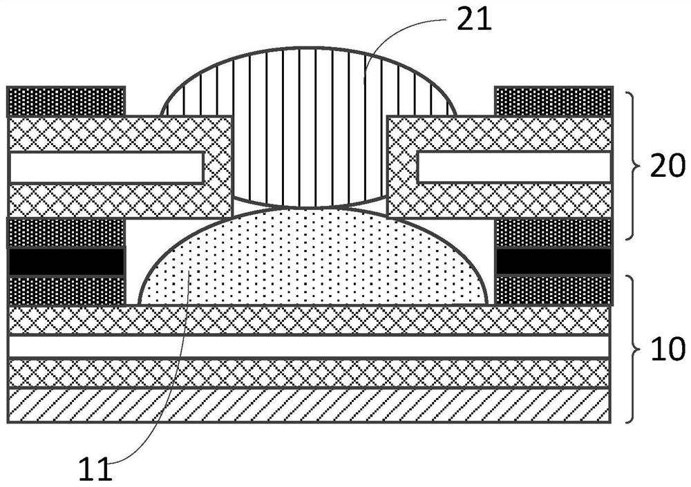
The invention provides a flexible circuit board, a manufacturing method thereof and a display device. The flexible circuit board comprises a main board and a small board, the main board is provided with at least one first welding area for exposing a part of a first conductive layer, the small board is provided with at least one second welding area for exposing a part of a second conductive layer, the second welding area comprises a welding hole, the orthographic projection of the second welding area on the mainboard is at least partially overlapped with the first welding area, and the first conductive layer and the second conductive layer are connected through a welding structure. The welding structure comprises: a first layer of welding flux which is located on the first conductive layer part exposed by the first welding area; a second layer of welding flux which is located on the part, exposed out of the second welding area, of the second conducting layer, wherein at least part of the second layer of welding flux is welded and fixed to the first layer of welding flux through the welding hole; and a high-melting-point connecting piece, wherein one end of the high-melting-point connecting piece is located in the first layer of welding flux, the other end of the high-melting-point connecting piece is located in the second layer of welding flux in the welding hole, and the melting point of the high-melting-point connecting piece is higher than that of the first layer of welding flux and that of the second layer of welding flux. According to the flexible circuit board, the manufacturing method thereof and the display device, the welding quality and the welding yield of the circuit board can be improved.

Description

technical field [0001] The invention relates to the technical field of circuit boards, in particular to a flexible circuit board, a manufacturing method thereof, and a display device. Background technique [0002] In the related art, a flexible printed circuit (FPC) is a highly reliable and excellent flexible printed circuit board made of polyimide or polyester film as the base material. [0003] In the display module using the FMLOC (Flexible Multi-Layer On Cell, flexible multi-layer touch structure) process, the TP (touch module) circuit is FOP bound to the M-FPC (main flexible circuit board) through the display screen. Fixed (FPC OnCOP Bonding) connection, from the perspective of cost performance, the M-FPC in the module of the FMLOC process flow will use the FPC of the multi-layer board stacking structure, such as the FPC of the 2+2 structure. [0004] The flexible circuit board of this multi-layer board stacking structure includes a main board and a small board. After ...

Claims


Application Information

Patent Timeline
IPC IPC(8): H05K1/11H05K1/02H05K1/14H05K3/34
CPCH05K1/111H05K1/0224H05K1/144H05K3/34H05K3/3494
Inventor 舒洋王天府汤强王景雷
Owner BOE TECH GRP CO LTD
Why Eureka
Try Eureka