System and method for data planarization

A data plane, data technology, used in static indicators, instruments, etc., can solve problems such as slow operation and large memory

Inactive Publication Date: 2004-01-28
OMNIVISION TECH INC
View PDF5 Cites 0 Cited by
  • Summary
  • Abstract
  • Description
  • Claims
  • Application Information

AI Technical Summary

Problems solved by technology

As a result, Urbanus' system requires a lot of memory and runs slowly

Method used


Image

  • System and method for data planarization
  • System and method for data planarization
  • System and method for data planarization

Examples


Embodiment Construction

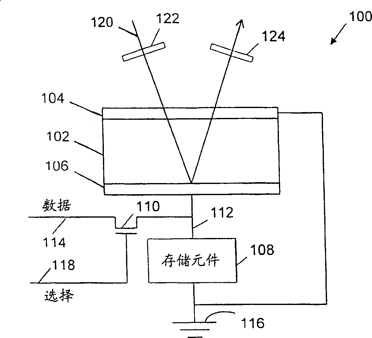
[0037] This patent application is related to the following pending U.S. patent applications, filed on the same date as this application and assigned to a common assignee, each of which is incorporated herein by reference in its entirety: Application in Off-Axis Projection Decentred Lens Groups in Display Driver Circuits, U.S. Patent No. 08 / 970,887, Matthew F. Bone and Donald Griffin Koch; Systems and Methods for Reducing Peak Current and Bandwidth Requirements in Display Driver Circuits, U.S. Patent No. 08 / 970,665, Raymond Pinkham, W. Spencer Worley, III, Edwin Lyle Hudson, and John Gray Campbell; System and Method for Improving Grayscale Performance of Displays Using Forced States, U.S. Patent No. 08 / 970,878, W. Spencer Worley, III, and Raymond Pinkham; and Reducing In-Display Driver Circuitry Internal Row Sequencer for Bandwidth and Peak Current Requirements, US Patent No. 08 / 970,443, Raymond Pinkham, W. Spancer Worley, III, Edwin Lyle Hudson, and John Gray Campbell.

[0038...


PUM


Abstract

A system and method for planarizing n-bit display data into m-bit data. The system includes a plurality of input terminals, a plurality of output terminals, and a first storage bank having a bit-depth less than m. In one embodiment, the first storage bank is a bi-directional shift register including a clock input terminal, for receiving a data shift signal, and a direction terminal for receiving a direction control signal. In a particular embodiment, the bi-directional shift register includes a plurality of flip-flops and a plurality of multiplexers, both arranged in a rectangular array of columns and rows. Optionally, the system includes a second storage bank, and data is shifted into one storage bank while data is being shifted out of the other storage bank.

Description

Background of the invention [0001] field of invention [0002] The present invention relates generally to electronic display drivers and, more particularly, to improved systems and methods for display data planarization. Description of background technology [0003] figure 1 A single pixel cell 100 of a typical liquid crystal display is shown. Pixel cell 100 includes a liquid crystal layer 102 contained between a transparent common electrode 104 and a pixel storage electrode 106 ; a storage element 108 ; and a switching transistor 110 . Storage element 108 is coupled to pixel storage electrode 106 at node 112 and to data input line 114 through switching transistor 110 . The storage element 108 is also coupled to the common voltage supply 116 as the common electrode 104 is coupled to the common voltage supply 116 (eg, ground). In response to a select signal on select line 118, which is coupled to the control terminal of switching transistor 110, memory element 108 reads...

Claims


Application Information

Patent Timeline
Patent Type & Authority Patents(China)
IPC IPC(8): G09G3/20G09G3/36
CPCG09G3/3648G09G3/2018
Inventor 威廉·T·韦瑟福德W·斯潘塞·沃利第三周永康
Owner OMNIVISION TECH INC
Why Eureka
Try Eureka