Nonvolatile memory device and forming method thereof

A non-volatile storage, non-device technology, applied in electrical components and other directions, can solve the problem that the performance of non-volatile memory needs to be improved, and achieve the effect of improving performance, avoiding leakage, and avoiding etching processes

Pending Publication Date: 2021-11-16
SEMICON MFG INT (SHANGHAI) CORP +1
View PDF0 Cites 0 Cited by
  • Summary
  • Abstract
  • Description
  • Claims
  • Application Information

AI Technical Summary

Problems solved by technology

[0004] However, the performance of non-volatile memories formed by existing processes needs to be improved

Method used


Image

  • Nonvolatile memory device and forming method thereof
  • Nonvolatile memory device and forming method thereof
  • Nonvolatile memory device and forming method thereof

Examples


Embodiment Construction

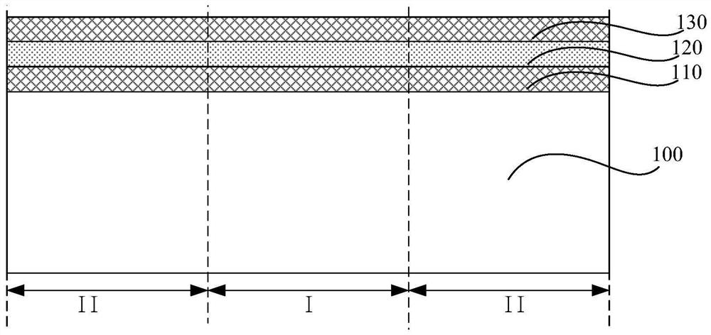
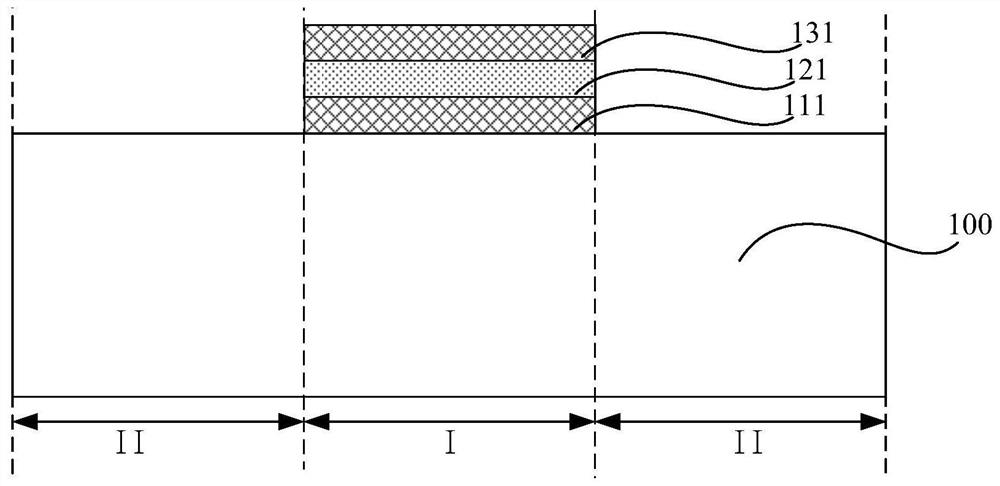
[0021] It can be known from the background art that the performance of the non-volatile memory formed by the existing technology needs to be improved. The reason why the device yield rate needs to be improved is analyzed in conjunction with a non-volatile memory forming method.

[0022] refer to Figure 1 to Figure 2 , the substrate can be divided into a device region I and a non-device region II, and a first electrode material layer 110, an insulating material layer 120 and a second electrode material layer 130 are sequentially formed on the substrate 100, wherein the first electrode material layer 110 and the The second electrode material layer 130 is a metal layer, and then, etch the first electrode material layer 110, the insulating material layer 120 and the second electrode material layer 130, and remove the first electrode material layer and the insulating material layer outside the device region 1. and the second electrode material layer to form a nonvolatile memory co...


PUM


Abstract

The invention discloses a nonvolatile memory device and a forming method thereof. The method comprises the steps of providing a substrate comprising a device region and a non-device region; sequentially forming a first electrode material layer and an insulating material layer on the substrate; forming a sacrificial layer on the insulating material layer, wherein the sacrificial layer covers the non-device region of the insulating material layer and exposes a device region of the insulating material layer; forming a second electrode on the exposed insulating material layer in the device region; and removing the sacrificial layer and the insulating material layer and the first electrode material layer in the non-device region, taking the residual insulating material layer as an insulating layer, and taking the residual first electrode material layer as a first electrode layer. The performance of the device is improved according to the method.

Description

technical field [0001] The invention relates to the field of semiconductor manufacturing, in particular to a non-volatile storage device and a forming method thereof. Background technique [0002] Memory is a memory device used to save information in modern information technology. It has a wide variety and is widely used. With the advancement of process technology and the growth of market demand, more and more high-density memories have been developed rapidly. [0003] RAM (Random Access Memory) has the problem of data loss after power failure during use. To overcome this problem, a variety of non-volatile memories have been designed and developed to retain data even when power is lost. Existing RAMs include PCRAM (Phase Change Memory), MRAM (Magnetic Memory), RRAM (Resistive Change Memory) and the like. [0004] However, the performance of the non-volatile memory formed by the existing process needs to be improved. Contents of the invention [0005] The problem to be ...

Claims


Application Information

Patent Timeline
Patent Type & Authority Applications(China)
IPC IPC(8): H01L45/00
CPCH10N70/821H10N70/061
Inventor 郑二虎
Owner SEMICON MFG INT (SHANGHAI) CORP
Why Eureka
Try Eureka