Array substrate and method for fabricating same

a technology of array substrate and substrate, applied in the field of array substrate, can solve the problems of increasing the number of manufacturing processes, and achieve the effects of reducing cost, simplifying the fabrication process, and improving the production efficiency of products

Inactive Publication Date: 2021-12-30
WUHAN CHINA STAR OPTOELECTRONICS TECH CO LTD
View PDF0 Cites 0 Cited by
  • Summary
  • Abstract
  • Description
  • Claims
  • Application Information

AI Technical Summary

Benefits of technology

The patent discusses a way of making an array substrate for displays. The process involves creating a layer of photoresist, patterning it with a laser, and then putting a layer of coating film on top of it. This new method allows for a more efficient and simplified process, improving production efficiency and reducing costs. The technical effect is the adjusted order of forming the coating film and the photoresist, which avoids the need for an etching process in the patterning treatment.

Problems solved by technology

However, the formation of the etching barrier layer requires an additional photolithography process, which increases the number of the manufacturing processes.

Method used


Image

  • Array substrate and method for fabricating same
  • Array substrate and method for fabricating same

Examples


Embodiment Construction

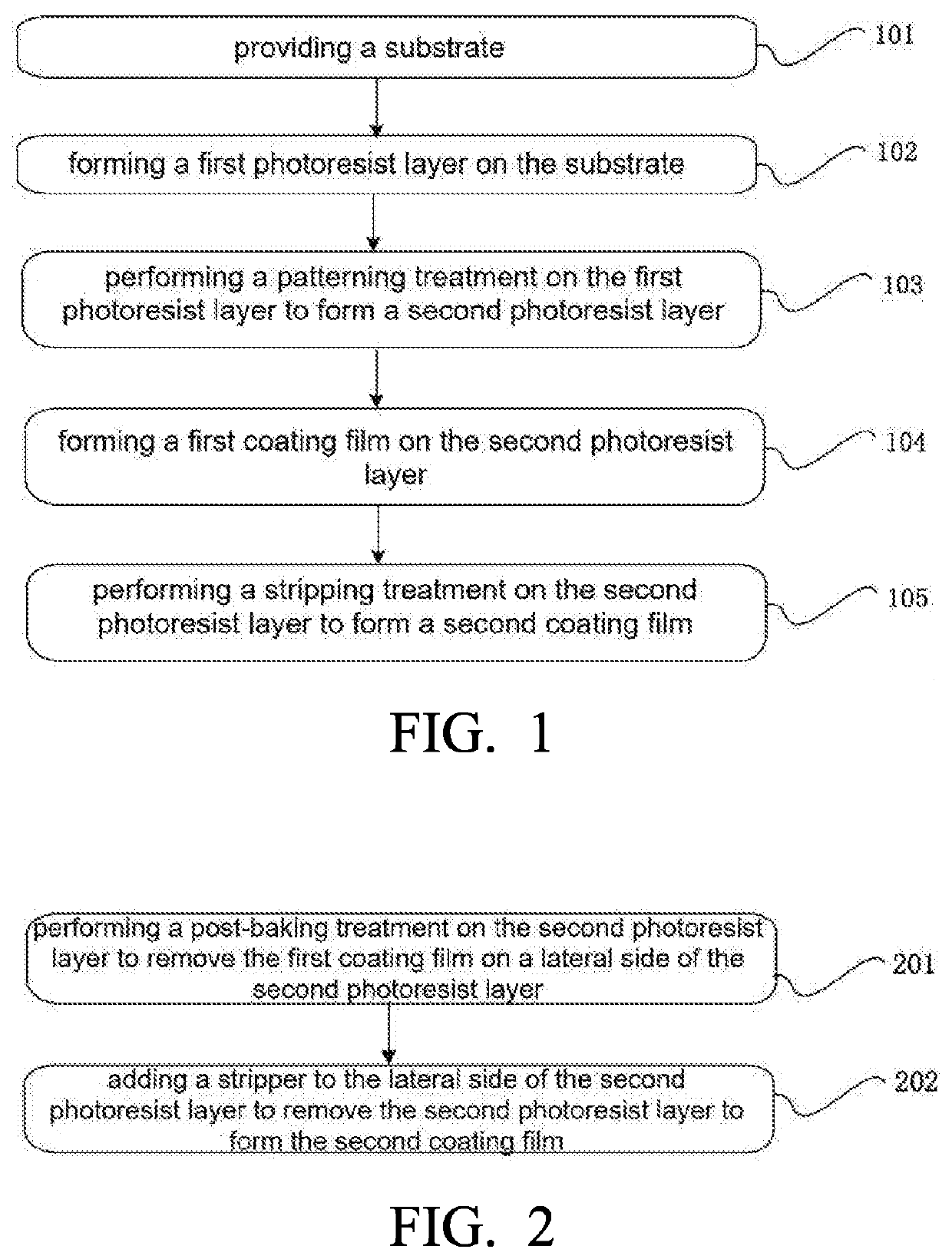
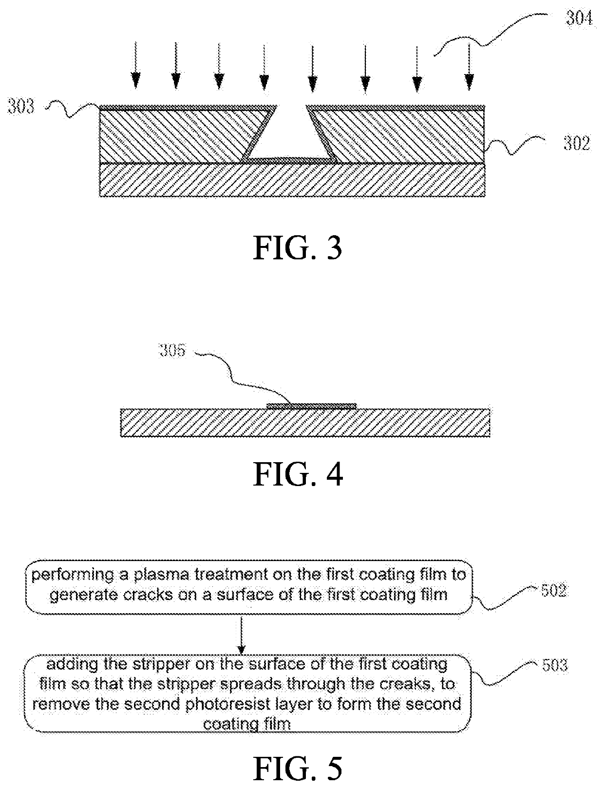
[0056]In the following, the technical solutions in the embodiments of the present disclosure will be clearly and completely described with reference to the drawings in the embodiments of the present disclosure. Obviously, the described embodiments are only a part of the embodiments of the present disclosure, but not all of the embodiments. Based on the embodiments of the present disclosure, all other embodiments obtained by those skilled in the art without creative work fall into the protection scope of the present disclosure.

[0057]In the following detailed description of the preferred embodiments, reference is made to the accompanying drawings which form a part hereof, and in which is shown by way of illustrating specific embodiments in which the disclosure may be practiced. In this regard, directional terminology, such as “top”, “bottom”, “front”, “back”, “left”, “right”, “inside”, “outside”, “side”, etc., is used with reference to the orientation of the figure(s) being described....


PUM

PropertyMeasurementUnit
temperatureaaaaaaaaaa

Abstract

An array substrate and a method for fabricating same are provided. Base on the existing process, the order of forming the coating film of the thin film transistor and forming the photoresist are adjusted. Thus, a patterning treatment can be directly performed on the first coating film, such that an etching process on the first coating film in the later can be avoided. Therefore, the etching process in the patterning treatment can be omitted, the fabrication process can be simplified, the production efficiency of the product can be improved, and the cost can be reduced.

Description

FIELD OF INVENTION[0001]The present disclosure relates to the field of display technologies, and more particularly, to an array substrate and a method for fabricating same.BACKGROUND OF INVENTION[0002]In the field of thin film transistor liquid crystal displays and active matrix organic light emitting diode (AMOLED) displays, oxide semiconductor material represented by indium gallium zincoxide (IGZO) have become hot spots. At present, the structure of IGZO thin film transistor array substrate mainly has three types: etching barrier type, back channel etching type, and coplanar type. The manufacturing process of the etch barrier type is relatively simple. The etching barrier layer on IGZO can protect the IGZO layer from being damaged when the source / drain electrode (S / D) is formed, such that the performance of IGZO can be enhanced. The material of the etching barrier layer is generally SiNx or SiOx. However, the formation of the etching barrier layer requires an additional photolitho...

Claims


Application Information

Patent Timeline
Patent Type & Authority Applications(United States)
IPC IPC(8): H01L27/12
CPCH01L27/1225H01L27/127H01L27/1288H01L21/0272H01L21/31133
Inventor LIU, HANCHEN
Owner WUHAN CHINA STAR OPTOELECTRONICS TECH CO LTD
Why Eureka
Try Eureka