Strain PMOSFET with surface stress modulation structure

A technology of surface stress and surface contact, which is applied in semiconductor/solid-state device manufacturing, electrical components, transistors, etc., can solve the problems of PMOSFET performance degradation, process complexity increase, process cost increase, etc., so as to suppress performance decline and decrease Complexity, effects of avoiding etch process

Active Publication Date: 2018-08-14
UNIV OF ELECTRONICS SCI & TECH OF CHINA
View PDF5 Cites 0 Cited by
  • Summary
  • Abstract
  • Description
  • Claims
  • Application Information

AI Technical Summary

Problems solved by technology

In the manufacture of CMOS integrated circuits, a tensile-strained silicon nitride capping layer is often deposited on the chip surface to improve the performance of NMOSFETs, but this capping layer often causes degradation of PMOSFET performance. figure 1 shown
In order to avoid the problem of PMOSFET performance degradation caused by the tensile strained silicon nitride capping layer, the industry generally adopts selective etching to remove the tensile strained silicon nitride capping layer on the surface of the PMOSFET to solve this problem. The CMOS cross-section of the strained silicon nitride capping layer is shown in figure 2 As shown, but this method also brings the problem of increased process complexity, which directly leads to an increase in process cost and a decrease in yield

Method used


Image

  • Strain PMOSFET with surface stress modulation structure
  • Strain PMOSFET with surface stress modulation structure
  • Strain PMOSFET with surface stress modulation structure

Examples


Embodiment Construction

[0034] The technical solution of the present invention will be described in detail below in conjunction with the accompanying drawings and embodiments.

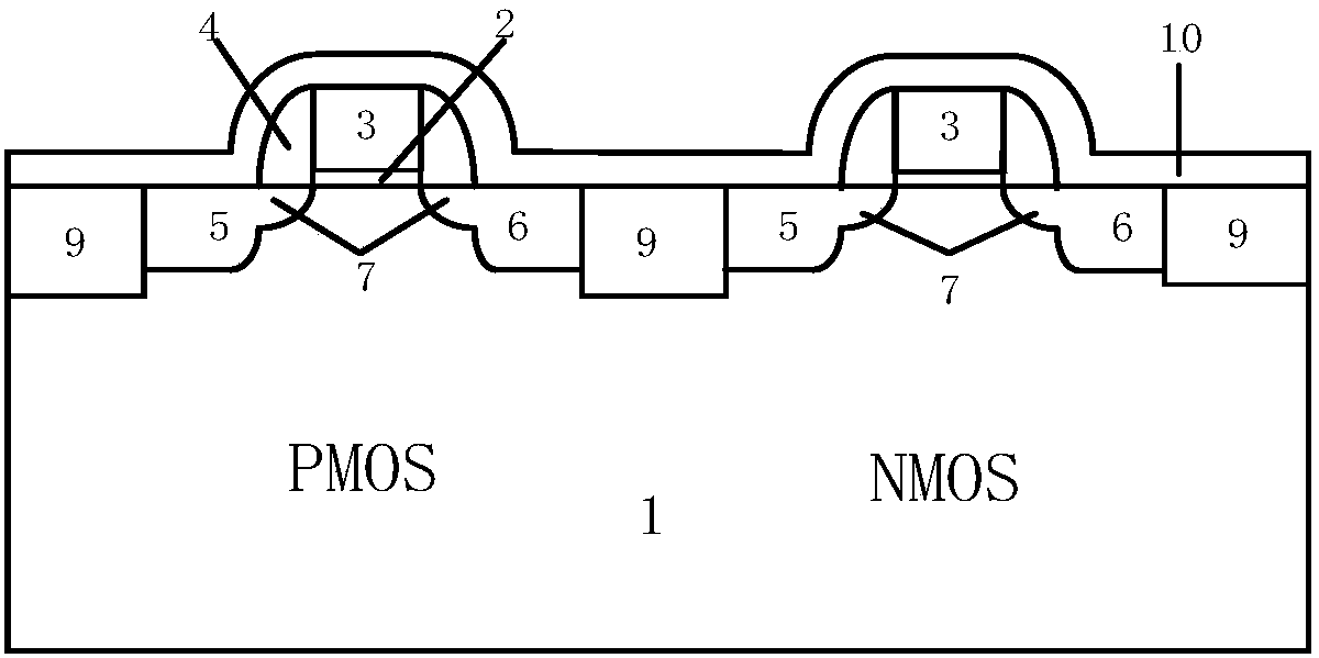
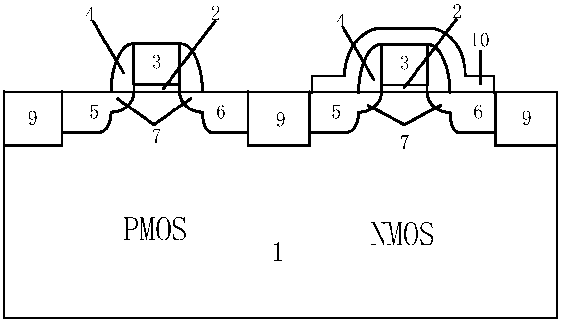
[0035] A strained PMOSFET with a surface stress modulation structure provided by the present invention includes a semiconductor substrate 1, a gate oxide layer 2, a gate 3, a source electrode, a drain electrode and two heavily doped regions, and the semiconductor substrate 1 starts from the bottom The gate oxide layer 2 and the gate 3 are arranged in sequence on the top. Two heavily doped regions are arranged in the semiconductor substrate 1 and located on both sides of the gate 3. The two heavily doped regions are the source region 5 and the drain region 6 respectively. The pole is arranged on the source region 5 and contacts the source region 5, the drain is arranged on the drain region 6 and contacts the drain region 6, and at least one insulating dielectric layer 8 is arranged on the semiconductor substrate 1, and the insu...


PUM


Abstract

The invention discloses a strain PMOSFET with a surface stress modulation structure, and belongs to the technical field of semiconductors. The strain PMOSFET comprises a semiconductor substrate, a gate oxide layer, a grid, a source, a drain and two heavily-doped regions, wherein the gate oxide layer and the gate are sequentially arranged on the semiconductor substrate from bottom to top; the two heavily-doped regions are arranged in the semiconductor substrate and are located on the two sides of the gate; the two heavily-doped regions are respectively a source region and a drain region; the source is arranged on the source region; the drain is arranged on the drain region; at least one insulating medium layer is further arranged on the semiconductor substrate; the insulating medium layer is arranged on one side, far away from the grid, of the heavily-doped region and is adjacent to the heavily-doped region; and a strain cap layer covers the upper surface of the whole device. Accordingto the strain PMOSFET, through a groove-shaped structure between the insulating medium layer and the grid, the decrease of the PMOSFET performance caused by a tensile strain silicon nitride cap layeris inhibited; and the strain PMOSFET is applied to a CMOS with the tensile strain silicon nitride cap layer, so that etching of the tensile strain cap layer on the surface of the PMOSFET is also avoided, and the process complexity is reduced.

Description

technical field [0001] The present invention relates to semiconductor technology, in particular to a strained metal oxide semiconductor field-effect transistor (MOSFET, metal oxide semiconductor Field-Effect Transistor), specifically a strained PMOSFET with a surface stress modulation structure. Background technique [0002] With the development of integrated circuits, the size of devices has become smaller and smaller, and the method of improving the performance of silicon-based MOSFETs (metal oxide semiconductor field effect transistors) by proportional reduction is subject to more and more physical and technological limitations. Under the small-scale manufacturing process, the strained silicon (Strained Silicon, SSi) technology can greatly improve the carrier mobility of the device through the introduction of stress, so that the output current of the device can be increased, thereby improving the performance of the circuit, and can Compatible with the existing Si process,...

Claims


Application Information

Patent Timeline
Patent Type & Authority Applications(China)
IPC IPC(8): H01L29/78H01L29/06H01L21/336
CPCH01L29/06H01L29/6659H01L29/78H01L29/7843H01L29/7833
Inventor 罗谦孟思远檀长桂王向展文厚东
Owner UNIV OF ELECTRONICS SCI & TECH OF CHINA
Why Eureka
Try Eureka