A kind of magnetic tunnel junction and its manufacturing method

A technology of a magnetic tunnel junction and a manufacturing method, which is applied in the manufacture/processing of electromagnetic devices, magnetic field-controlled resistors, digital memory information, etc. The effect of preventing device failure

Active Publication Date: 2021-05-25
JIANGSU LEUVEN INSTR CO LTD
View PDF11 Cites 0 Cited by
  • Summary
  • Abstract
  • Description
  • Claims
  • Application Information

AI Technical Summary

Problems solved by technology

Therefore, a more complicated etching method is required to realize it, and the etching process is relatively difficult.
[0005] In the etching method described in Patent Document 7, the damascene mosaic method is adopted, but due to the characteristics of the mosaic process such as the limitation of the dielectric etching morphology, it is difficult to obtain a high-density MTJ lattice
In addition, because the tunneling layer is very thin, the process of chemical mechanical polishing will cause material surface deformation or a small amount of metal residue, which may make the first magnetic layer and the second magnetic layer have conductive channels on the grinding surface, resulting in short circuits and device failure. fail

Method used


Image

  • A kind of magnetic tunnel junction and its manufacturing method
  • A kind of magnetic tunnel junction and its manufacturing method
  • A kind of magnetic tunnel junction and its manufacturing method

Examples


Embodiment Construction

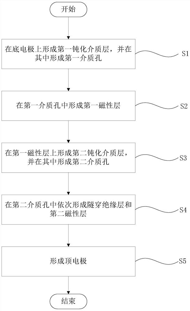
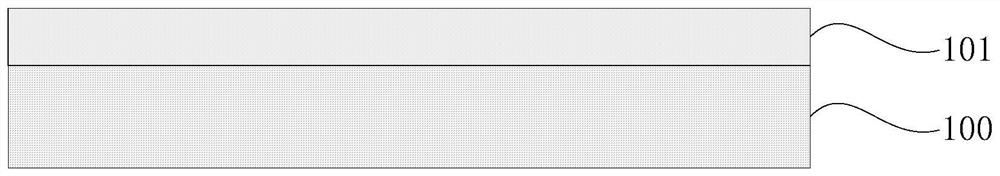
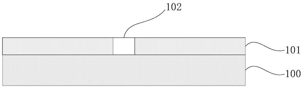
[0031] In order to make the purpose, technical solutions and advantages of the present invention clearer, the technical solutions in the embodiments of the present invention will be clearly and completely described below in conjunction with the accompanying drawings in the embodiments of the present invention. It should be understood that the specific The examples are only used to explain the present invention, not to limit the present invention. The described embodiments are only some, not all, embodiments of the present invention. Based on the embodiments of the present invention, all other embodiments obtained by persons of ordinary skill in the art without making creative efforts belong to the protection scope of the present invention.

[0032] In the description of the present invention, it should be noted that the orientations or positional relationships indicated by the terms "up", "down", "steep", "inclined" etc. are based on the orientations or positional relationship...


PUM

PropertyMeasurementUnit
thicknessaaaaaaaaaa
thicknessaaaaaaaaaa
thicknessaaaaaaaaaa

Abstract

The invention discloses a magnetic tunnel junction and a manufacturing method thereof. The magnetic tunnel junction manufacturing method includes the following steps: a first dielectric hole forming step, forming a first passivation dielectric layer on the bottom electrode, and forming a first dielectric hole in the first passivation dielectric layer; a first magnetic layer forming step, Form the first magnetic layer in the first dielectric hole, make the top surface of the first magnetic layer and the top surface of the first passivation medium layer be in the same plane; the second dielectric hole forming step, in the first magnetic layer forming a second passivation dielectric layer on the second passivation dielectric layer, and forming a second dielectric hole in the second passivation dielectric layer; forming a tunneling insulating layer and a second magnetic layer, forming a tunneling insulating layer sequentially in the second dielectric hole and a second magnetic layer; and a top electrode forming step of forming a top electrode on the second magnetic layer. The magnetic tunnel junction and the manufacturing method thereof of the present invention effectively reduce the difficulty of the etching process of the magnetic tunnel junction, and effectively improve the reliability and yield of the device.

Description

technical field [0001] The invention relates to the field of magnetic random access memory, in particular to a magnetic tunnel junction and a manufacturing method thereof. Background technique [0002] Magnetic random access memory (MRAM) is a non-volatile magnetic random access memory, which has the high-speed read and write capabilities of static random access memory (SRAM) and the high integration of dynamic random access memory (DRAM). And it can basically be written repeatedly indefinitely, which is one of the mainstream products in the field of wafer manufacturing industry. [0003] Magnetic tunnel junction (MTJ) is the core structure of MRAM, which is composed of fixed layer, non-magnetic isolation layer and free layer. Among them, the fixed layer is thicker, has stronger magnetism, and the magnetic moment is not easy to reverse, while the free layer is thinner, weaker in magnetism, and the magnetic moment is easy to reverse. According to the parallel and antiparall...

Claims


Application Information

Patent Timeline
Patent Type & Authority Patents(China)
IPC IPC(8): G11C11/16H01L43/08H01L43/12
CPCG11C11/161H10N50/01H10N50/10
Inventor 许开东
Owner JIANGSU LEUVEN INSTR CO LTD
Why Eureka
Try Eureka