
Chip pad structure, chip, wafer and chip pad structure manufacturing method

A technology of chip pads and manufacturing methods, applied in semiconductor/solid-state device manufacturing, semiconductor/solid-state device components, semiconductor devices, etc., can solve problems such as chip function failure, avoid virtual soldering, reduce the risk of function failure, The effect of improving reliability

Active Publication Date: 2022-03-01
BEIJING SMARTCHIP MICROELECTRONICS TECH COMPANY +3
View PDF0 Cites 0 Cited by
  • Summary
  • Abstract
  • Description
  • Claims
  • Application Information

AI Technical Summary

Problems solved by technology

When in use, the flip chip will encounter the problem of function failure

Method used


Image

  • Chip pad structure, chip, wafer and chip pad structure manufacturing method
  • Chip pad structure, chip, wafer and chip pad structure manufacturing method
  • Chip pad structure, chip, wafer and chip pad structure manufacturing method

Examples


Embodiment 1

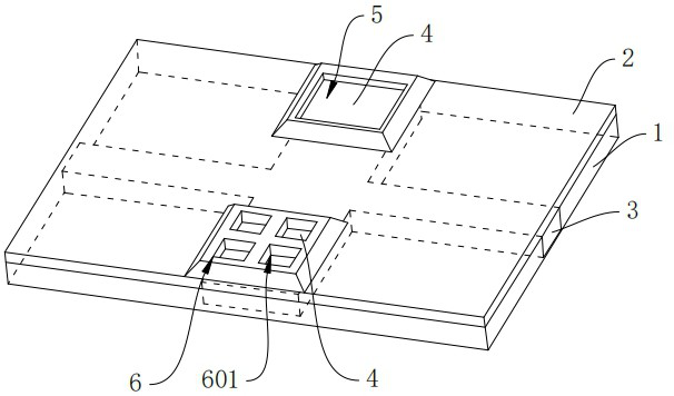
[0062] figure 1 It is a schematic diagram of the chip pad structure provided by an embodiment of the present invention, such as figure 1 As shown, the chip pad structure includes:

[0063] The first insulating layer 1 has grooves;

[0064] The first metal layer 3 is filled in the groove of the first insulating layer 1, and the first metal layer 3 is connected with the internal circuit of the chip to form a conductive channel;

[0065] The second metal layer 4 is formed on the first metal layer 3, and the second metal layer 4 has a pad area for connecting the chip to an external device;

[0066] The second insulating layer 2 covers at least the part of the second metal layer 4 outside the pad area and the first metal layer 3;

[0067] The pad area includes a test pad area 5 and a gold bump pad area 6; the gold bump pad area 6 includes a plurality of sub-pad areas. Among them, the test pad area 5 is used for connecting pads for CP testing after the chip is manufactured, and ...

Embodiment 2

[0101] image 3 It is a schematic diagram of the chip pad structure provided by another embodiment of the present invention, such as image 3 As shown, the chip pad structure includes:

[0102] The first insulating layer 1 has grooves;

[0103] The first metal layer 3 is filled in the groove of the first insulating layer 1, and the first metal layer 3 is connected with the internal circuit of the chip to form a conductive channel;

[0104] The second metal layer 4 is formed on the first metal layer 3, and the second metal layer 4 has a pad area for connecting the chip to an external device;

[0105] The second insulating layer 2 covers at least the part of the second metal layer 4 outside the pad area and the first metal layer 3;

[0106] The pad area includes a test pad area 5 and a gold bump pad area 6; the gold bump pad area 6 includes a plurality of sub-pad areas. Among them, the test pad area 5 is used for connecting pads for CP testing after the chip is manufactured,...

Embodiment 3

[0140] Figure 5 It is a schematic diagram of the chip pad structure provided by another embodiment of the present invention, such as image 3 As shown, the chip pad structure includes:

[0141] The first insulating layer 1 has grooves;

[0142] The first metal layer 3 is filled in the groove of the first insulating layer 1, and the first metal layer 3 is connected with the internal circuit of the chip to form a conductive channel;

[0143] The second metal layer 4 is formed on the first metal layer 3, and the second metal layer 4 has a pad area for connecting the chip to an external device;

[0144] The second insulating layer 2 covers at least the part of the second metal layer 4 outside the pad area and the first metal layer 3;

[0145] The pad area includes a test pad area 5 and a gold bump pad area 6; the gold bump pad area 6 includes a plurality of sub-pad areas. Among them, the test pad area 5 is used for connecting pads for CP testing after the chip is manufactured...


PUM


Abstract

The invention provides a chip pad structure, a chip, a wafer and a method for manufacturing the chip pad structure, belonging to the field of chips. The chip pad structure includes: a first insulating layer, including a groove; a first metal layer, filled in the groove, and the first metal layer is connected with the internal circuit of the chip to form a conductive channel; a second metal layer, formed on the On a metal layer, including the pad area where the chip is connected to external devices; the second insulating layer covers at least the part of the second metal layer outside the pad area and the first metal layer; the pad area includes a test pad area and the gold bump pad area; the gold bump pad area includes a plurality of sub-pad areas. There are no pits on the surface of the gold bump formed by electroplating on the gold bump pad area, and at the same time, it can ensure the effective contact between the gold bump and the gold bump pad, reducing the risk of functional failure due to weak soldering after chip packaging risk.

Description

technical field [0001] The invention relates to the field of chips, in particular to a chip pad structure, a chip, a wafer and a method for manufacturing the chip pad structure. Background technique [0002] In chip packaging technology, the conventional chip packaging process includes two key processes of die bonding and wire bonding, while flip chip (Flip-Chip, FC for short) technology combines the above two key processes into one. It realizes the interconnection between the chip and the packaging substrate (or circuit board) directly through the bumps arranged in an array on the chip. Because the chip is buckled upside down on the packaging substrate, which is opposite to the placement direction of the conventional packaged chip, it is called Flip-Chip. When in use, flip chips suffer from functional failures. Contents of the invention [0003] The purpose of the embodiments of the present invention is to provide a chip pad structure, a chip, a wafer, and a method for ...

Claims


Application Information

Patent Timeline
Patent Type & Authority Patents(China)
IPC IPC(8): H01L23/488H01L21/60
CPCH01L24/06H01L24/03H01L2224/0401H01L2224/03H01L2224/0361H01L2224/06515
Inventor 张贺丰林杰李建强李延王文赫
Owner BEIJING SMARTCHIP MICROELECTRONICS TECH COMPANY
Learn More