Welding device and method for electronic component

A technology of electronic components and welding devices, which is applied in the direction of assembling printed circuits, auxiliary devices, welding equipment, etc. of electrical components, which can solve problems such as low welding efficiency, solder cracks, and prone to stress tendency, so as to improve welding efficiency and prevent cracks , the effect of less prone to stress

Pending Publication Date: 2021-12-03
广东愈焜健康科技有限公司
View PDF8 Cites 2 Cited by
  • Summary
  • Abstract
  • Description
  • Claims
  • Application Information

AI Technical Summary

Problems solved by technology

[0003] 1) The welding process is carried out in the air, rich in more oxygen, more oxygen will remain in the weld, prone to stress tendencies, and then easily lead to cracks in the solder;
[0004] 2) Every time an electronic component is welded, the solder joint needs to be preheated, and the welding efficiency is low

Method used


Image

  • Welding device and method for electronic component
  • Welding device and method for electronic component
  • Welding device and method for electronic component

Examples


Embodiment 1

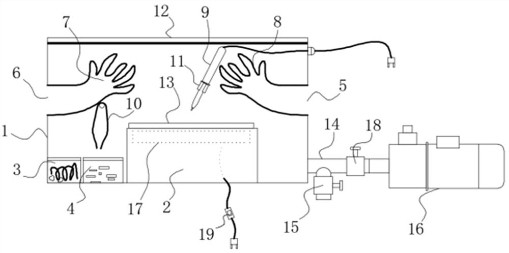
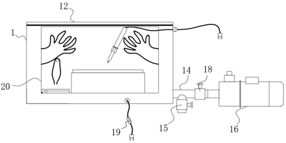
[0041] Please refer to figure 1 and figure 2 , the embodiment of the present invention provides a welding device for electronic components, including a vacuum pump 16 and a sealed welding operation box 1 that can observe all the scenes inside from the outside. The top of the welding operation box 1 is provided with a sealing cover 12;

[0042] The welding operation box 1 is communicated with the first end of a three-way pipe 14, the second end of the three-way pipe 14 is provided with the first on-off gas valve 15, and the third end is provided with the second on-off gas valve 18 and is connected with the vacuum pump 16. suction port connection;

[0043] Soldering operation box 1 is provided with electric soldering iron 9, electronic component placement box 4, solder placement box 3, tweezers 10, silicone glove Ⅰ 8, silicone glove Ⅱ 7 and PCB placement seat 2, PCB placement seat 2 has a built-in infrared heater 17, The power plug of the infrared heater 17 and the power plug...

Embodiment 2

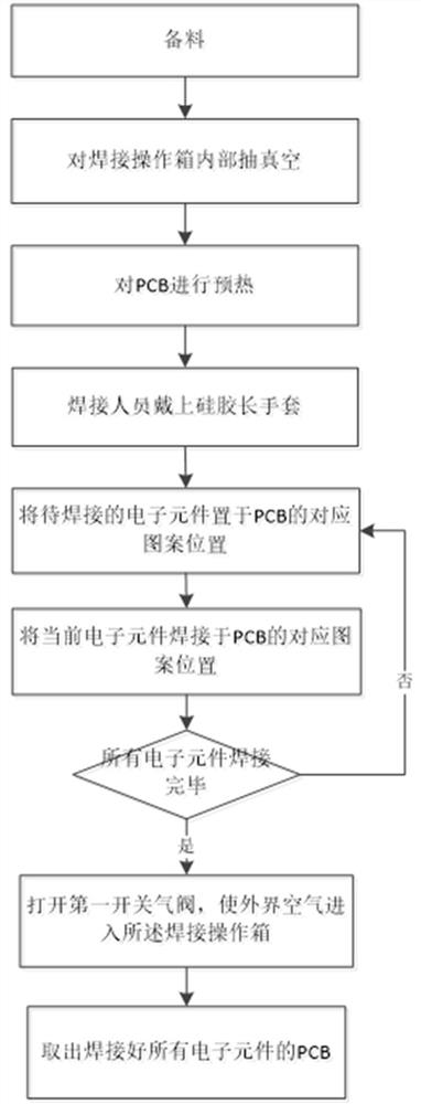
[0052] Please refer to figure 1 , figure 2 and image 3 , the embodiment of the present invention provides an electronic component welding method based on the welding device described in embodiment 1, specifically comprising the following steps:

[0053] S1. Open the sealing cover 12, place the required solder in the solder placement box 3, place the electronic components to be soldered in the electronic component placement box 4, place the PCB to be soldered on the PCB placement seat 2, and then cover Upper sealing cover 12;

[0054] S2, open the second switching gas valve 18, close the first switching gas valve 15, utilize the vacuum pump 16 to vacuumize the inside of the welding operation box 1, and then close the second switching gas valve 18;

[0055] S3. Connect the electric soldering iron 9 and the infrared heater 17 to the power supply, and preheat the PCB through the infrared heater 17. After reaching 120~130°C, cut off the power supply of the infrared heater 17, ...


PUM


Abstract

The invention discloses a welding device and method for an electronic component, and relates to the technical field of electronic component welding. The adopted welding method adopts the designed unique electronic component welding device, the welding time is shortened, the reliable structure of a welding spot part can be ensured, and the electronic component and the corresponding pattern of the PCB can be fully and correctly connected. In the welding process of the electronic component, a vacuum environment is created, oxygen does not exist in a welding seam, the stress tendency is not prone to occurring, and welding flux is not prone to generating cracks. In the preheating process, the whole PCB is preheated at a time, due to the fact that the PCB is in the vacuum environment, the PCB can keep the preheating temperature for a long time, and the preheating time is greatly shortened.

Description

technical field [0001] The invention relates to the technical field of electronic component welding, in particular to a welding device and method for electronic components. Background technique [0002] Soldering has traditionally been widely used as a method of mounting electronic components on PCBs. At present, the items required for manual soldering of electronic components include solder and electric soldering iron. In order to avoid unfavorable situations such as false soldering, the electric soldering iron is often first touched to the spot to be soldered for about 2 seconds, and then the solder is sent to the spot to be soldered. The current manual soldering method for electronic components has the following defects: [0003] 1) The welding process is carried out in the air, rich in more oxygen, more oxygen will remain in the weld, prone to stress tendencies, and then easily lead to cracks in the solder; [0004] 2) Every time an electronic component is welded, it i...

Claims


Application Information

Patent Timeline
Patent Type & Authority Applications(China)
IPC IPC(8): B23K3/00B23K3/08H05K3/34B23K101/42
CPCB23K3/00B23K3/08H05K3/34B23K2101/42
Inventor 陆韦亨
Owner 广东愈焜健康科技有限公司
Why Eureka
Try Eureka