Improved silica stain test structures and methods therefor

A technology for testing structures and silica, which is applied in the direction of optical testing flaws/defects, semiconductor/solid-state device manufacturing, semiconductor/solid-state device testing/measurement, etc. It can solve the inconvenience of process engineers and other problems, and achieve easy-to-observe, increase the amount of dissolution, easy to create effects

Inactive Publication Date: 2004-02-04
SIEMENS AG +1
View PDF0 Cites 0 Cited by
  • Summary
  • Abstract
  • Description
  • Claims
  • Application Information

AI Technical Summary

Problems solved by technology

[0008] Those skilled in the art will appreciate that the additional processing steps required to detect and / or measure stains formed on prior art silicon monitoring test structures have a number of disadvantages
At a minimum, additional processing would inconvenience the process engineer, who would have to do extra work before the presence and / or amount of silica stain could be detected
Additionally additional processing introduces additional complications, usually measured in additional time and / or expense required

Method used


Image

  • Improved silica stain test structures and methods therefor
  • Improved silica stain test structures and methods therefor
  • Improved silica stain test structures and methods therefor

Examples


Embodiment Construction

[0021] The present invention will be described in detail below with reference to several exemplary embodiments provided in the drawings. In the following description, some specific details are described in order to fully understand the present invention. However, it is obvious that for those skilled in the art, the present invention can be implemented without some or all of these specific details. On the other hand, the well-known process steps and / or structures are not described in detail, which is to make it easier to understand the present invention.

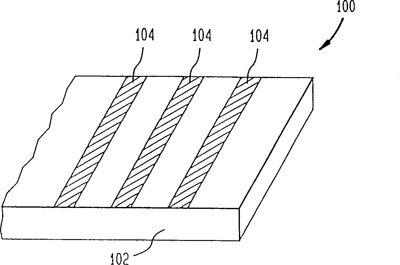
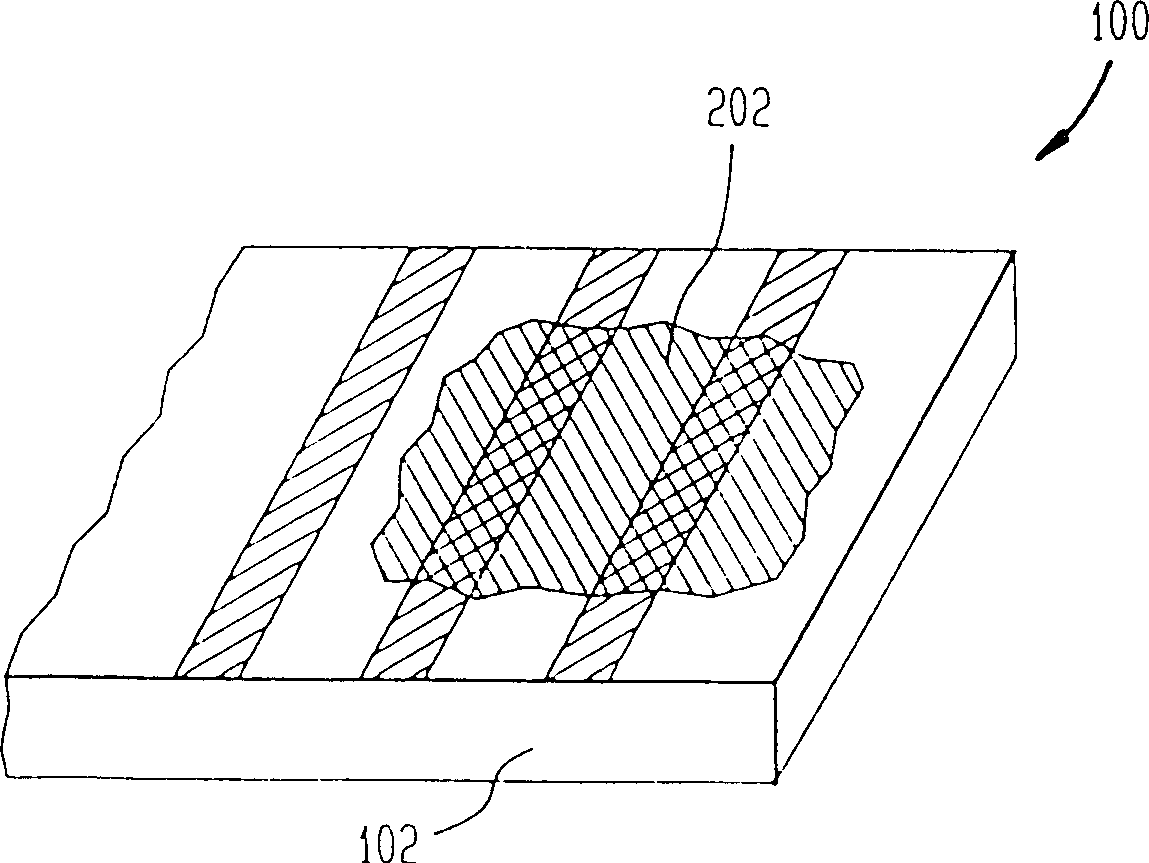
[0022] According to an embodiment of the present invention, an inventive silica stain formation technology is provided, which can significantly increase the amount of silicon dissolved in the cleaning process. By adding silicon hydrates, the silica stains remaining on the test structure after drying will be significantly enlarged and / or thickened, so that the use of ordinary optical monitoring equipment (eg, using a conventional ...


PUM

PropertyMeasurementUnit
critical dimensionaaaaaaaaaa
thicknessaaaaaaaaaa

Abstract

A method for forming silica stain on a substrate to facilitate monitoring of the silica stain during integrated circuit manufacture. The method includes providing a silica stain test structure which has a silicon substrate, a hydrophilic silicon dioxide containing layer disposed above the silicon substrate, and a plurality of cavities formed in the silicon substrate through the silicon dioxide containing layer. The cavities have hydrophobic sidewalls. The method also includes exposing the silica stain test structure to deionized water, and drying the silica stain test structure to form the silica stain on the silicon dioxide containing layer.

Description

Technical field [0001] The invention relates to the manufacture of integrated circuits. In particular, the present invention relates to a method for forming silica stains on a substrate during an integrated circuit manufacturing process, and a silica stain test structure and a manufacturing method thereof. Background technique [0002] In the production of semiconductor integrated circuits, wet chemical reagents are often used during wafer processing. For example, some processing procedures require the patterned wafer to be immersed in a wet, liquid chemical reagent for etching. After the exposed part of the wafer is etched away by the wet chemical reagent, the wafer is taken out, cleaned with deionized water, and then dried. [0003] After cleaning and drying, it was found that silica stains sometimes appeared on the wafer surface. Silica stains are produced by the dissolved silicon dioxide in the cleaning solution, which re-deposit on the wafer surface during the drying process...

Claims


Application Information

Patent Timeline
Patent Type & Authority Patents(China)
IPC IPC(8): G01N21/88G01N21/93G01N21/956H01L21/304H01L21/306H01L21/66H01L23/544H01L27/10
CPCH01L22/34H01L21/02
Inventor 拉斯·阿恩特苏珊·科恩罗纳德·霍耶科琳·斯内夫利
Owner SIEMENS AG
Why Eureka
Try Eureka