


Quick Research
Generate reliable direction feasibility study reports for your R&D in just a few steps.

Technical Q&A
Discover and master advanced knowledge NOW. Basics, ideas, possibilities, all at once.

Find Solutions
As an expert in R&D theories, this can generate solutions to your technical problems instantly.

Evaluate Feasibility
Analyze your overall solution with one click, know your potential R&D risks in advance.

Monitor Landscape
Get weekly tech updates, stay abreast of the latest tech innovations and key insights.
Sesquioxide transparent ceramic scintillation screen for X-ray imaging detector and application of screen
An imaging detector and sesquioxide technology, applied in the field of X-ray imaging, can solve the problems of limited selection of scintillators, inability to accurately optimize X-ray absorption of different energies, etc., to achieve easy preparation in large areas, improve imaging effects, and optimize absorption The effect of efficiency
- Summary
- Abstract
- Description
- Claims
- Application Information
AI Technical Summary
Problems solved by technology
Method used
Image

Examples
Embodiment 1
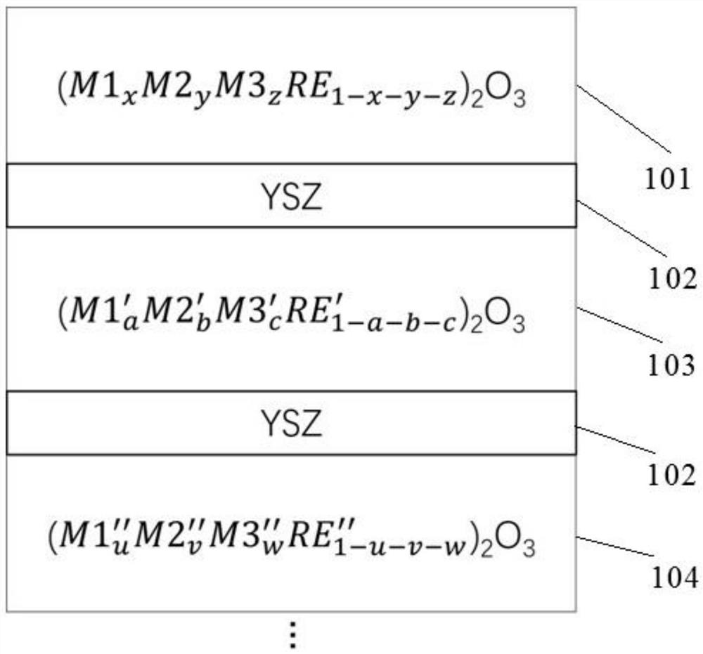
[0055] (Gd 0.2 Y 0.75 Tb 0.05 ) 2 o 3 (200μm) / YSZ(200μm) / (Lu 0.85 La 0.1 Eu 0.05 ) 2 o 3 (600μm) scintillation screen
[0056] The upper scintillator is 200μm thick (Gd 0.2 Y 0.75 Tb 0.05 ) 2 o 3 , the split layer is 200μm YSZ, and the lower scintillator is 600μm (Lu 0.85 La 0.1 Eu 0.05 ) 2 o 3 , the cross section is 100×100mm 2 , Formed in one piece with transparent ceramic technology.
[0057] The scintillation vial of this embodiment was tested with a microscope objective lens NikonCFIPlanFluor, Numerical Aperture numerical aperture NA=0.13, X-ray source as W target (160KeV), and the system spatial resolution reached 10 μm. The above imaging system performs CT imaging of mixed materials of metal materials gold (Z=79) and lead (Z=82) with similar densities, which can better distinguish the two materials.
Embodiment 2
[0059] (Lu 0.1 Gd 0.1 sc 0.75 Tb 0.05 ) 2 o 3 (1mm) / (Lu 0.85 Gd 0.1 Eu 0.05 ) 2 o 3 (2mm) flickering screen
[0060] The upper scintillator is 1 mm thick (Lu 0.1 Gd 0.1 sc 0.75 Tb 0.05 ) 2 o 3 , without split layer, the lower scintillator is 2mm thick (Lu 0.85 Gd 0.1 Eu 0.05 ) 2 o 3 , the cross section is 100×100mm 2 , the upper scintillator and the lower scintillator are formed separately by transparent ceramic technology, and then combined to prepare.
Embodiment 3
[0062] (Lu 0.1 Gd 0.1 Y 0.75 T m 0.05 ) 2 o 3 (1mm) / YSZ(400μm)(Lu 0.5 La 0.35 Gd 0.1 Tb 0.05 ) 2 o 3 (2mm) / YSZ(400μm) / (Lu 0.8 La 0.05 sc 0.1 Eu 0.05 ) 2 o 3 (2.5mm)
[0063] The first layer of scintillator is 1mm thick (Lu 0.1 Gd 0.1 Y 0.75 T m 0.05 ) 2 o 3 , the first split layer is 400μm thick YSZ, the second scintillator is 2mm thick (Lu 0.5 La 0.35 Gd 0.1 Tb 0.05 ) 2 o 3 , the second split layer is 400μm thick YSZ, the third layer scintillator is 2.5mm thick (Lu 0.8 La 0.05 sc 0.1 Eu 0.05 ) 2 o 3 The cross section is 3000×3000mm 2 , It is prepared by integral molding of transparent ceramic technology.
PUM
| Property | Measurement | Unit |
|---|---|---|
| thickness | aaaaa | aaaaa |
| thickness | aaaaa | aaaaa |
| thickness | aaaaa | aaaaa |
Abstract
Description
Claims
Application Information
 - R&D Engineer
- R&D Manager
- IP Professional
- Industry Leading Data Capabilities
- Powerful AI technology
- Patent DNA Extraction
Browse by: Latest US Patents, China's latest patents, Technical Efficacy Thesaurus, Application Domain, Technology Topic, Popular Technical Reports.
© 2024 PatSnap. All rights reserved.Legal|Privacy policy|Modern Slavery Act Transparency Statement|Sitemap|About US| Contact US: help@patsnap.com