

Method for removing photoresist
A photoresist and wet degumming technology, used in optics, optomechanical equipment, photosensitive material processing, etc., can solve problems such as difficult to meet, surface damage of semiconductor materials, etc., and achieve the effect of fast and effective removal
- Summary
- Abstract
- Description
- Claims
- Application Information
AI Technical Summary
Problems solved by technology
Method used
Image

Examples
Embodiment Construction
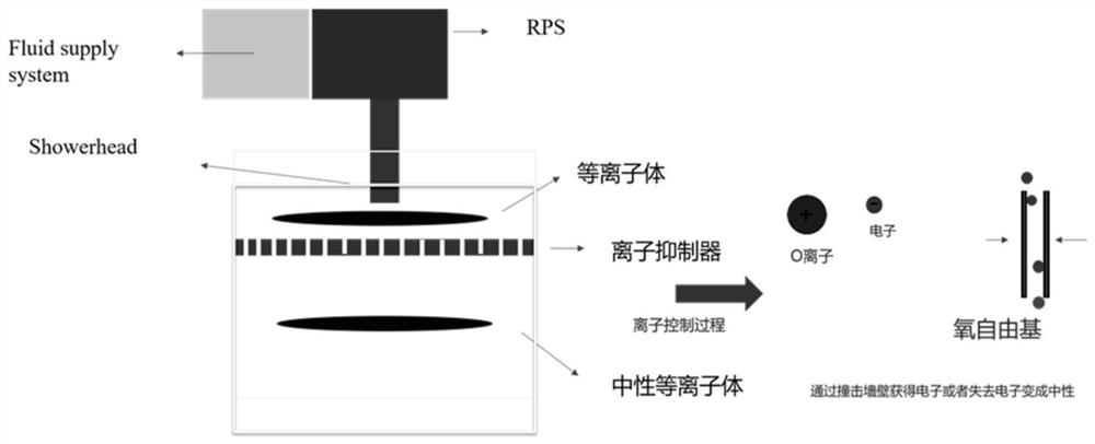
[0019] The existing plasma deglue process uses oxygen, water vapor, carbon dioxide and other oxygen-containing gases as the working gas to excite it to generate plasma and collide with the photoresist layer to produce volatile reactants to realize the removal of the photoresist layer. Purpose. However, the photoresist removal effect of the existing plasma deglue process is still difficult to be satisfied; on the other hand, the plasma will cause damage to the surface of the semiconductor material. The charge damage caused by the battery is becoming more and more unacceptable.
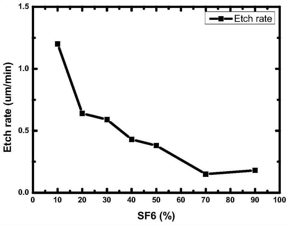
[0020] In order to solve this problem, the idea of the present invention is to adopt the SF within 20% 6 As an auxiliary gas in the plasma degumming process, it removes charged particles in the generated plasma.
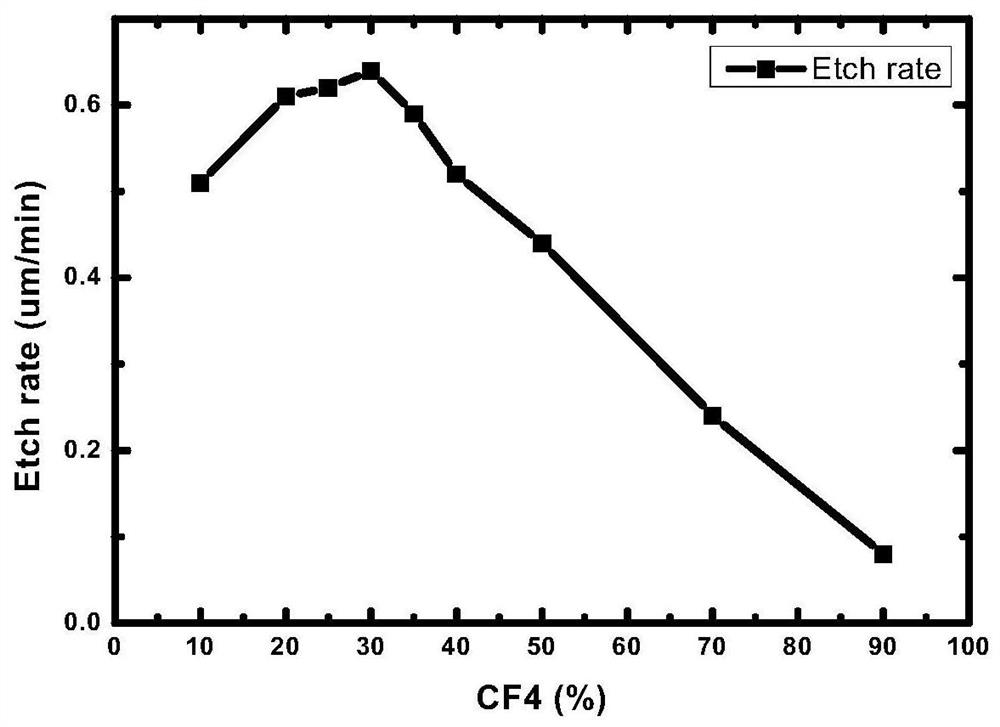
[0021] In order to improve the removal rate of photoresist, the prior art often adds H to the working gas 2 、CH 4 , NH 3 and other auxiliary gases, among which the most commonly used an...
PUM
| Property | Measurement | Unit |
|---|---|---|
| thickness | aaaaa | aaaaa |
Abstract
Description
Claims
Application Information