Supercharge Your Innovation With Domain-Expert AI Agents!

LED photoelectric device and preparation method thereof

A technology for optoelectronic devices and electrodes, applied in the field of LED optoelectronic devices and their preparation, can solve the problems of reduced size of RGB optoelectronic devices, low efficiency of a single RGB chip, thick LED optoelectronic devices, etc. rate effect

Pending Publication Date: 2021-12-28
HUIZHOU VISION NEW TECH CO LTD
View PDF0 Cites 0 Cited by
  • Summary
  • Abstract
  • Description
  • Claims
  • Application Information

AI Technical Summary

Problems solved by technology

[0003] Among them, the efficiency of transferring a single RGB chip with a die bonder is low, and the die bonder uses thimbles and suction nozzles to grab individual RGB chips one by one, and places the single RGB chip on the package bracket, and the die bonder can operate the chip The size of one side is generally greater than 80 microns, which limits the further reduction of the size of RGB optoelectronic devices, and thus limits the size of the final optoelectronic devices, and also limits the further reduction of the cost of optoelectronic devices
[0004] At the same time, in order to avoid damage to the RGB chip during the die-bonding process, the RGB chip usually needs to include a supporting substrate. The supporting substrate is usually an epitaxial growth substrate, so the thickness of the chip is relatively thick, usually greater than 100 microns. Therefore, LED optoelectronic devices The structure includes: packaging bracket, RGB chip, packaging adhesive layer, this structure will cause thicker LED optoelectronic devices

Method used

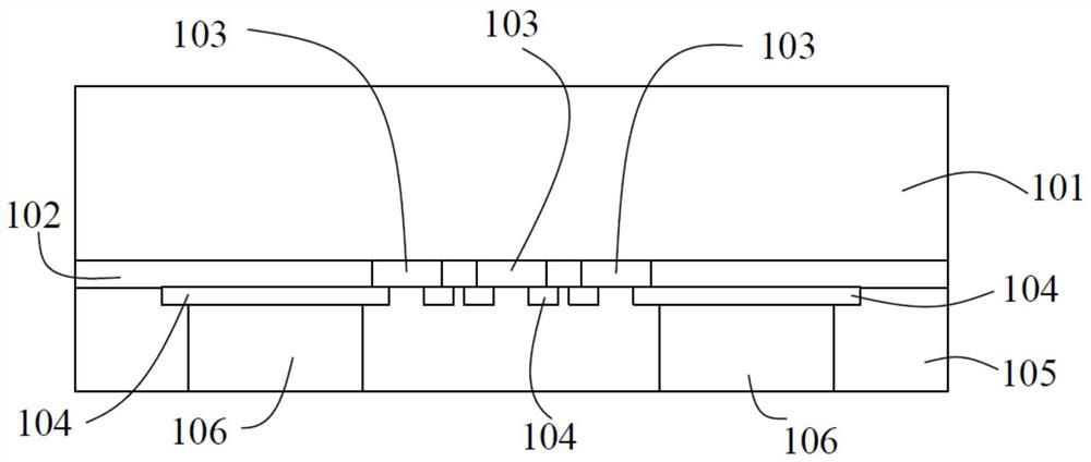

Image

  • LED photoelectric device and preparation method thereof
  • LED photoelectric device and preparation method thereof
  • LED photoelectric device and preparation method thereof

Examples


Embodiment Construction

[0036] The technical solutions in the embodiments of the present application will be clearly and completely described below in conjunction with the drawings in the embodiments of the present application. Apparently, the described embodiments are only some of the embodiments of this application, not all of them. Based on the embodiments in this application, all other embodiments obtained by those skilled in the art without making creative efforts belong to the protection scope of this application.

[0037] Reference herein to an "embodiment" means that a particular feature, structure, or characteristic described in connection with the embodiment can be included in at least one embodiment of the present application. The occurrences of this phrase in various places in the specification are not necessarily all referring to the same embodiment, nor are separate or alternative embodiments mutually exclusive of other embodiments. It is understood explicitly and implicitly by those s...


PUM


Abstract

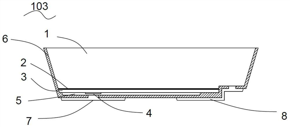
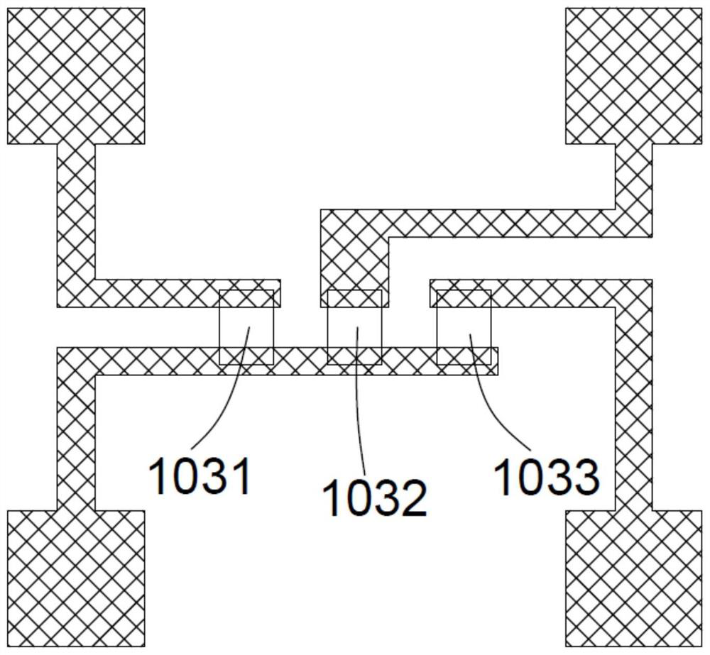
The invention discloses an LED photoelectric device and a preparation method thereof. The LED photoelectric device comprises: a substrate; an adhesion layer adhered to the substrate, wherein a plurality of RGB chips are adhered in the adhesion layer, the light-emitting surfaces of the RGB chips vertically face the substrate, one side, deviating from the substrate, of each RGB chip comprises an electrode, and the electrodes are exposed out of the adhesion layer; a metal circuit layer arranged on the side, away from the substrate, of the adhesion layer, and electrically connected with the electrodes; an insulating layer arranged on one side, deviating from the adhesive layer, of the metal circuit layer; and a metal bonding pad penetrating through the insulating layer to be electrically connected with the metal circuit layer. Compared with the prior art, the size of an LED photoelectric chip is greatly reduced, when the LED photoelectric chip is used for an LED display panel, the resolution ratio of the LED display panel can be improved, meanwhile, the thickness of the LED display panel is reduced, the image quality and attractiveness of the LED display panel are improved, and the use value of an LED photoelectric device is improved.

Description

technical field [0001] The present application relates to the field of LED technology, in particular to an LED optoelectronic device and a preparation method thereof. Background technique [0002] For the production of LED optoelectronic devices, at present, a single RGB chip is bonded to the packaging bracket one by one by a die-bonding machine. Depending on the structure of the chip, it may be necessary to use a wire bonder to complete the electrical connection, then mold the packaging glue, and finally cut it. Independent LED optoelectronic device. [0003] Among them, the efficiency of transferring a single RGB chip with a die bonder is low, and the die bonder uses thimbles and suction nozzles to grab individual RGB chips one by one, and places the single RGB chip on the package bracket, and the die bonder can operate the chip The size of one side is generally greater than 80 microns, which limits the further reduction of the size of the RGB optoelectronic device, and t...

Claims


Application Information

Patent Timeline
IPC IPC(8): H01L25/075H01L33/06H01L33/62G09F9/33
CPCH01L25/0753H01L33/06H01L33/62G09F9/33
Inventor 桑永昌李健林
Owner HUIZHOU VISION NEW TECH CO LTD
Features
  • R&D
  • Intellectual Property
  • Life Sciences
  • Materials
  • Tech Scout
  • Unparalleled Data Quality
  • Higher Quality Content
  • 60% Fewer Hallucinations
Learn More