Millimeter wave surface-mounted airtight packaging structure and packaging method

A hermetic packaging and millimeter wave technology, applied in the direction of electrical components, electric solid devices, circuits, etc., can solve the problems of large transmission loss in the millimeter wave frequency band, difficult to promote, complex structure, etc., to avoid the deterioration of microwave signal quality, The effect of reducing the assembly process and simplifying the operation

Pending Publication Date: 2021-12-31
THE 13TH RES INST OF CHINA ELECTRONICS TECH GRP CORP
View PDF0 Cites 3 Cited by
  • Summary
  • Abstract
  • Description
  • Claims
  • Application Information

AI Technical Summary

Problems solved by technology

The disadvantage of these structures is that the structure is complex and the cost is high; or due to the large parasitic parameters, the transmission loss in the millimeter wave band is large, the performance is seriously degraded, and it is even unusable.
As a result, it is difficult to popularize these structural packages in chip applications with frequencies higher than 40 GHz

Method used


Image

  • Millimeter wave surface-mounted airtight packaging structure and packaging method
  • Millimeter wave surface-mounted airtight packaging structure and packaging method
  • Millimeter wave surface-mounted airtight packaging structure and packaging method

Examples


Embodiment Construction

[0035] In order to make the technical problems, technical solutions and beneficial effects to be solved by the present invention clearer, the present invention will be further described in detail below in conjunction with the accompanying drawings and embodiments. It should be understood that the specific embodiments described here are only used to explain the present invention, not to limit the present invention.

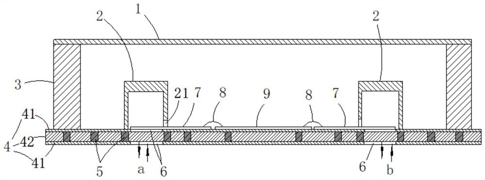
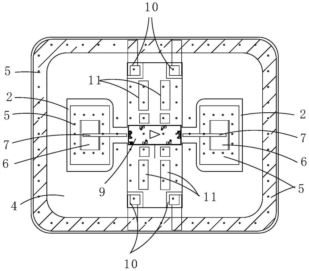
[0036] Please also refer to figure 1 and figure 2 , the millimeter-wave surface-mount hermetic packaging structure provided by the present invention will now be described. The millimeter-wave surface-mounted hermetic packaging structure includes a package housing, a chip 9 and two waveguide cavity reflection structures 2. The package housing includes a bottom plate 4, a welding frame 3 arranged on the bottom plate 4, and a package on the top of the welding frame 3. The metal cover plate 1, the bottom plate 4 includes a dielectric plate 42 and a grounding plate 4...


PUM


Abstract

The invention provides a millimeter wave surface-mounted airtight packaging structure and packaging method, and belongs to the technical field of microwave packaging. The millimeter wave surface-mounted airtight packaging structure comprises a packaging shell, a chip and waveguide cavity reflection structures, wherein the packaging shell comprises a bottom plate, a welding frame and a metal cover plate, and the bottom plate comprises a dielectric plate and grounding plates arranged on the upper surface and the lower surface of the dielectric plate respectively; the chip is arranged on the grounding plate on the upper surface; the waveguide cavity reflection structures are arranged on the grounding plate on the upper surface and are respectively arranged on the left side and the right side of the chip, and the waveguide cavity reflection structures are connected with the chip through microstrip line probes and bonding wires; and the part, which directly faces the grounding plate, of the cavity of each waveguide cavity reflection structure is provided with a window, and the two windows respectively form a radio frequency input port and a radio frequency output port. According to the invention, through structure adjustment, chip airtight packaging can be expanded to a millimeter wave frequency band range, the requirements of packaging precision and airtight packaging can be met, batch production is facilitated, the production efficiency is greatly improved, and the production cost is reduced.

Description

technical field [0001] The invention belongs to the technical field of microwave packaging, and in particular relates to a millimeter-wave surface-mounted hermetic packaging structure and a packaging method. Background technique [0002] With the continuous growth of communication application requirements, the existing spectrum resources are becoming increasingly tight, and the increase in communication capacity also requires a wider operating bandwidth, so the operating frequency is gradually increased to the millimeter wave frequency band. The demand for non-destructive testing in security inspections has promoted the development of terahertz technology, and more and more millimeter-wave frequency band chips are widely used. Since bare chips cannot be directly used for design in most scenarios, conventional applications are to encapsulate bare chips in plastic or use metal or ceramic hermetic packaging. [0003] Microwave circuits with a frequency lower than 30GHz already...

Claims


Application Information

Patent Timeline
Patent Type & Authority Applications(China)
IPC IPC(8): H01L23/498H01L23/66H01L21/48
CPCH01L23/49894H01L23/66H01L21/4846
Inventor 周彪孔令甲彭同辉要志宏许问前韩玉朝王建李德才
Owner THE 13TH RES INST OF CHINA ELECTRONICS TECH GRP CORP
Why Eureka
Try Eureka