Array substrate, manufacturing method thereof and display panel

An array substrate and manufacturing method technology, applied in the field of display, can solve problems such as inability to level pits and protrusions, fluctuations in the thickness of the array substrate, and limited flattening ability of the planarization layer, so as to reduce thickness, improve flatness, and improve flatness the effect of the effect

Pending Publication Date: 2021-12-31
HEFEI VISIONOX TECH CO LTD
View PDF0 Cites 0 Cited by
  • Summary
  • Abstract
  • Description
  • Claims
  • Application Information

AI Technical Summary

Problems solved by technology

[0003] The LTPS array is formed by patterning and stacking different functional layers, and the flattening ability of the flattening layer in the array film layer is limited, that is, the flat organic glue has certain fluidity and viscosity, and will flow down, but it cannot make the pits and protrusions are completely leveled, resulting in thickness fluctuations of the array substrate under the pixel area
In the prior art, the planarization effect is improved by increasing the thickness of the planarization layer, which will result in an increase in the thickness of the screen

Method used


Image

  • Array substrate, manufacturing method thereof and display panel
  • Array substrate, manufacturing method thereof and display panel
  • Array substrate, manufacturing method thereof and display panel

Examples


Embodiment Construction

[0049] The present invention will be further described in detail below in conjunction with the accompanying drawings and embodiments. It should be understood that the specific embodiments described here are only used to explain the present invention, but not to limit the present invention. In addition, it should be noted that, for the convenience of description, only some structures related to the present invention are shown in the drawings but not all structures.

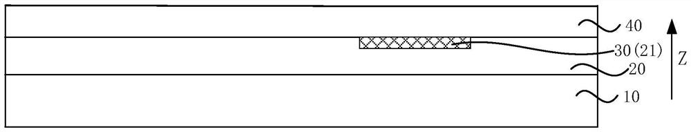
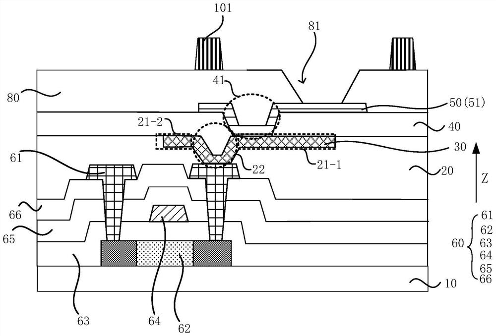
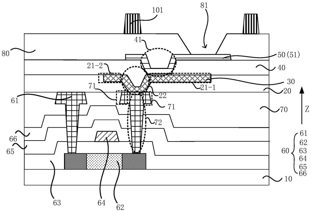
[0050]An embodiment of the present invention provides an array substrate. figure 1 It is a schematic cross-sectional structure diagram of an array substrate provided by an embodiment of the present invention. The array substrate can be set in the display panel. The array substrate includes a base 10 , and a first planarization layer 20 , a first conductive layer 30 and a second planarization layer 40 located on the base 10 .

[0051] Wherein, the first planarization layer 20 is located between the substrate 10 a...


PUM

PropertyMeasurementUnit
thicknessaaaaaaaaaa

Abstract

The embodiment of the invention discloses an array substrate, a manufacturing method thereof and a display panel. The array substrate comprises a substrate, and a first planarization layer, a first conductive layer and a second planarization layer which are positioned on the substrate. The first planarization layer is located between the substrate and the second planarization layer; the first conductive layer is located between the first planarization layer and the second planarization layer; a first groove is formed in one side, close to the second planarization layer, of the first planarization layer; the first conductive layer is partially or completely located in the first groove, so that the flatness of the side, away from the substrate, of the first conductive layer and the flatness of the side, away from the substrate, of the first planarization layer are improved. According to the technical scheme provided by the embodiment of the invention, the planarization effect can be improved, the thickness of the planarization layer is reduced, and the planarization effect does not depend on the thickness of the planarization layer.

Description

technical field [0001] The present invention relates to the field of display technology, in particular to an array substrate, a manufacturing method thereof, and a display panel. Background technique [0002] In an actively driven display device, in order to realize active driving, a Low Temperature Poly-Silicon (LTPS for short) array substrate design is currently used. [0003] The LTPS array is formed by patterning and stacking different functional layers, and the flattening ability of the flattening layer in the array film layer is limited, that is, the flat organic glue has certain fluidity and viscosity, and will flow down, but it cannot make the pits and the protrusions are completely leveled, resulting in thickness fluctuations of the array substrate under the pixel area. In the prior art, the planarization effect is improved by increasing the thickness of the planarization layer, which will increase the thickness of the screen body. Contents of the invention [0...

Claims


Application Information

Patent Timeline
Patent Type & Authority Applications(China)
IPC IPC(8): H01L27/12H01L21/77H01L27/15H01L27/32
CPCH01L27/124H01L27/1244H01L27/1248H01L27/1259H01L27/156H10K59/12H10K59/131
Inventor 朱微曹方义肖一鸣姚远赵理朱雪婧
Owner HEFEI VISIONOX TECH CO LTD
Why Eureka
Try Eureka