Switch control circuit and method for preventing voltage drop caused by overlarge load
A switch control circuit and voltage drop technology, applied in the direction of electronic switches, circuits, electrical components, etc., can solve problems such as inflexibility, increased cost, and design incompatibility, and achieve the effect of reducing hardware costs and suppressing load instantaneous current
- Summary
- Abstract
- Description
- Claims
- Application Information
AI Technical Summary
Problems solved by technology
Method used
Image
Examples
Embodiment 1
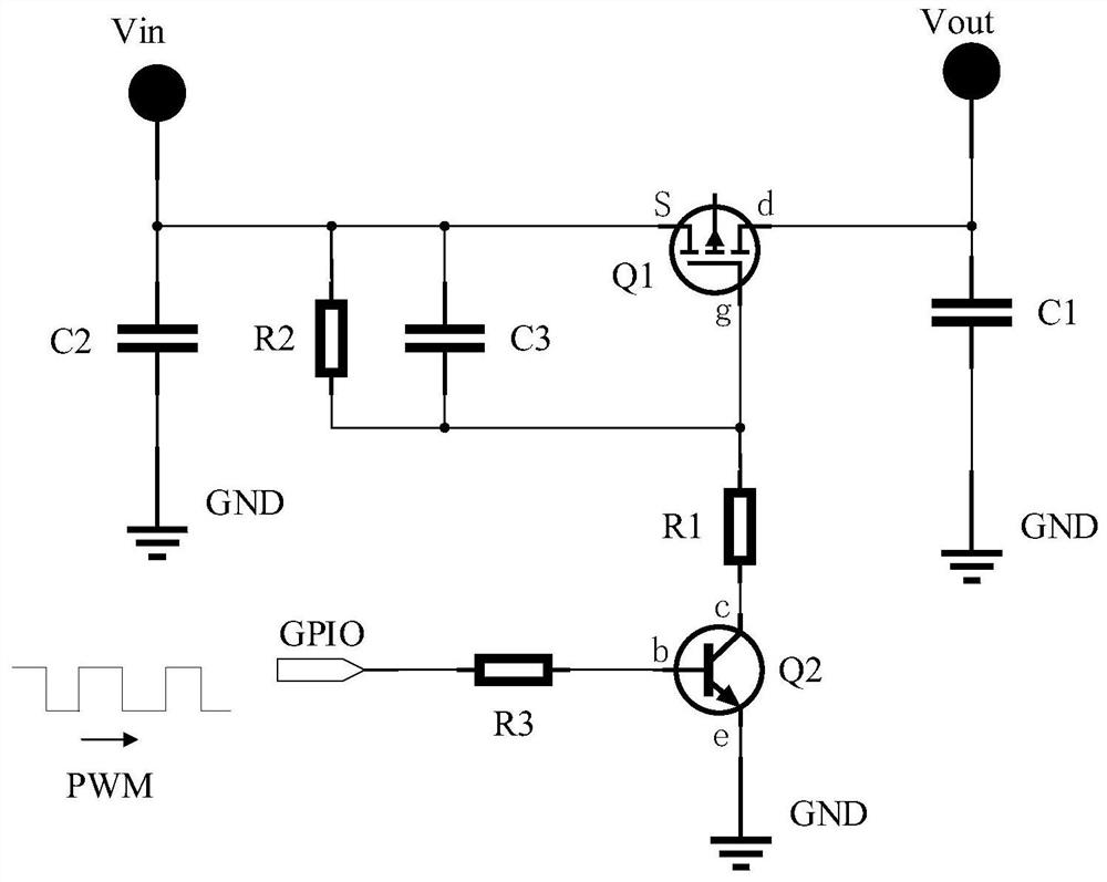
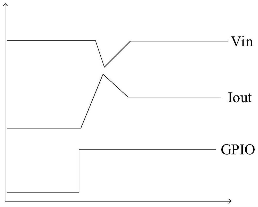
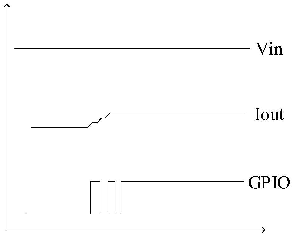
[0050] Please refer to Figure 1 to Figure 3 , Embodiment 1 of the present invention is:
[0051] A switch control circuit for preventing voltage drop caused by excessive load includes a switch circuit and a control circuit.
[0052] like figure 1As shown, the switching circuit includes a PMOS transistor Q1, a first capacitor C1, a second capacitor C2, a third capacitor C3, a first resistor R1, and a second resistor R2. The source s of the PMOS transistor Q1 is simultaneously connected to the power supply input terminal Vin, the second capacitor One end of the second capacitor C2, one end of the third capacitor C3, and one end of the second resistor R2 are electrically connected, the drain d of the PMOS transistor Q1 is electrically connected to one end of the first capacitor C1 and the power supply output terminal Vout at the same time, and the gate of the PMOS transistor Q1 The pole g is electrically connected to one end of the first resistor R1, the other end of the secon...
Embodiment 2
[0062] Please refer to Figure 4 , the second embodiment of the present invention is:
[0063] A switch control method for preventing voltage drop caused by excessive load, comprising the following steps:
[0064] Receive the input voltage of the power supply input terminal and the PWM signal of the signal control terminal;
[0065] When the PWM signal is at a high level, the switching transistor is turned on, which makes the PMOS tube turn on, and the input voltage is output to the load device connected to the output terminal of the power supply. On the contrary, when the PWM signal is at a low level, the switching transistor is turned off, so that the PMOS tube is turned off. , the input voltage stops outputting, and this cycle continues until the load instantaneous current Iout of the load device reaches the operating current, and the signal control terminal maintains a high-level signal.
[0066] To sum up, the present invention provides a switch control circuit and meth...
PUM
| Property | Measurement | Unit |
|---|---|---|
| electrical resistance | aaaaa | aaaaa |
| electrical resistance | aaaaa | aaaaa |
| electrical resistance | aaaaa | aaaaa |
Abstract
Description
Claims
Application Information


