PLED driving chip and display device
A drive chip, GND technology, applied in the direction of static indicators, instruments, etc., can solve the problems of unreasonable power supply pin layout, excessive display brightness reduction, large ITO voltage drop, etc., to reduce impedance, reduce impedance, The effect of reducing the brightness reduction
- Summary
- Abstract
- Description
- Claims
- Application Information
AI Technical Summary
Problems solved by technology
Method used
Image

Examples
Embodiment Construction
[0018] The specific implementation manners of the present invention will be further described in detail below in conjunction with the accompanying drawings and embodiments. The following examples are used to illustrate the present invention, but are not intended to limit the scope of the present invention.
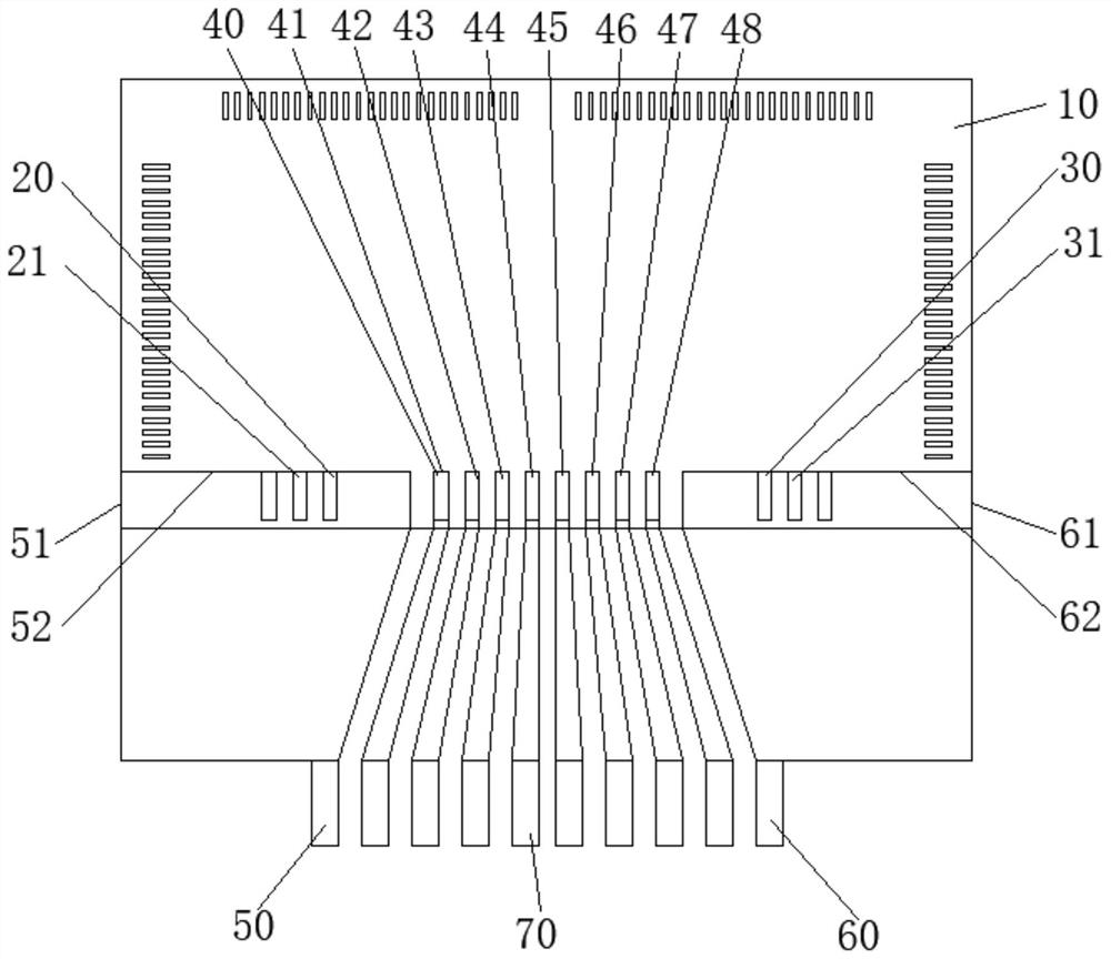
[0019] Please refer to figure 1 , the embodiment of the present invention provides a PLED driver chip, including a substrate 10, a VDD (DeviceVoltage, the positive pole of the working voltage of the chip) interface 20, a GND (Ground, negative pole of the working voltage of the chip) interface 30, a signal line interface 40, an external VDD connection line 50, external GND connection line 60, external signal line connection line 70 and GND terminal (not shown). The GND terminal is located in the substrate 10, the VDD interface 20, the GND interface 30, and the signal line interface 40 are all arranged on the outer surface of the substrate 10, the external VDD connection li...
PUM
 Abstract
Description
Claims
Application Information