
A double vacuum chamber wafer proton irradiation device and irradiation method

A technology of proton irradiation and vacuum chamber, which is applied in the direction of irradiation devices, circuits, electrical components, etc., can solve the problem that insulated gate bipolar transistors lack deep proton irradiation production technology, cannot be matched with IGBT chips, and their performance cannot be compared with imported chips. Ratio and other issues, to achieve the effect of reducing radiation damage, small energy dispersion, and large capacity

Active Publication Date: 2022-05-10
国核铀业发展有限责任公司 +2
View PDF0 Cites 0 Cited by
  • Summary
  • Abstract
  • Description
  • Claims
  • Application Information

AI Technical Summary

Problems solved by technology

[0003] However, the performance of domestic insulated gate bipolar transistor (IGBT) and other power chips cannot be compared with imported chips due to the lack of deep proton irradiation production technology
In addition, the current domestically produced fast recovery diode (FRD) chips are also unable to achieve the performance of a softness factor above 2 due to the lack of deep proton irradiation technology, and cannot be used in conjunction with IGBT chips in fields such as electric vehicles

Method used


Image

  • A double vacuum chamber wafer proton irradiation device and irradiation method
  • A double vacuum chamber wafer proton irradiation device and irradiation method

Examples


Embodiment Construction

[0043] In order to make the purposes, technical solutions and advantages of the embodiments of the present invention clearer, the technical solutions in the embodiments of the present invention will be clearly and completely described below with reference to the accompanying drawings in the embodiments of the present invention. Obviously, the described embodiments These are some embodiments of the present invention, but not all embodiments. Based on the embodiments of the present invention, all other embodiments obtained by those of ordinary skill in the art without creative efforts shall fall within the protection scope of the present invention.

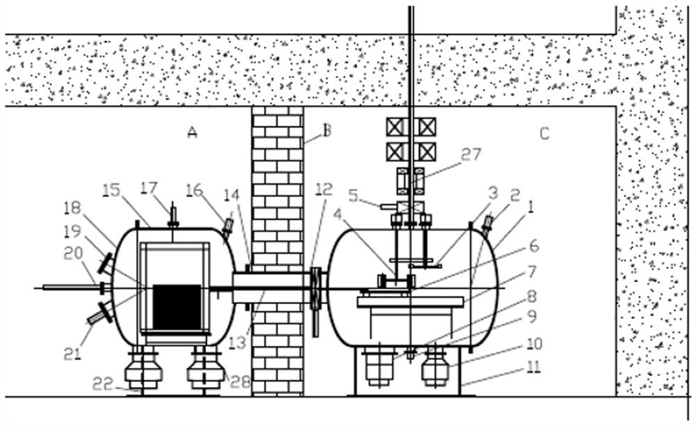
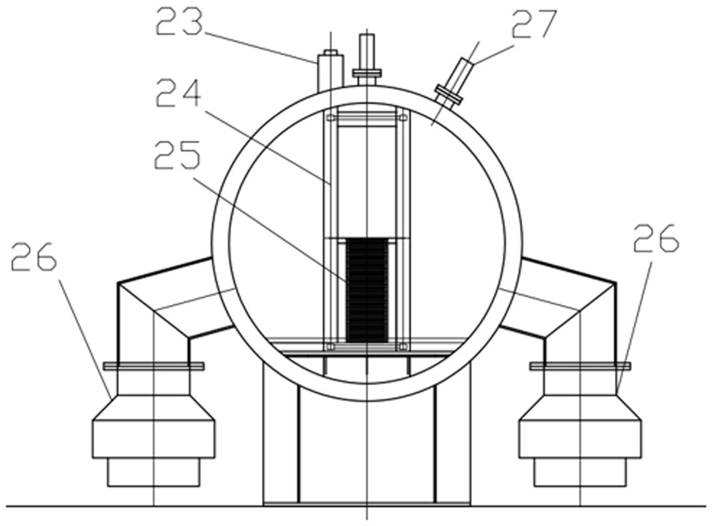
[0044] figure 1 Shown is a side view of the dual vacuum chamber wafer proton irradiation apparatus of the present invention. figure 2 Shown is a cross-sectional view of the wafer-changing vacuum chamber of the dual-vacuum chamber wafer proton irradiation device of the present invention.

[0045] see figure 1 . The double vacuum...


PUM


Abstract

The invention provides a double vacuum chamber wafer proton irradiation device and an irradiation method. The double vacuum chamber wafer proton irradiation device includes: a wafer irradiation vacuum chamber and a wafer replacement vacuum chamber. The wafer irradiation The vacuum chamber and the film-changing vacuum chamber are connected through the connecting vacuum section; the connecting vacuum section is provided with a shielding wall; the wafer irradiation vacuum chamber is set in the irradiation hall, and the film-changing vacuum chamber is set in the irradiation front hall , the shielding wall seals and separates the irradiation hall from the irradiation vestibule. The irradiation device is very suitable for high-energy proton irradiation, which is conducive to greatly reducing the radiation damage suffered by workers, can realize uniform irradiation of wafers, improves irradiation quality, has a large capacity, improves production efficiency, and ensures wafer The round tray is transported smoothly, effectively in place, and will not activate the atmosphere, which helps to improve the irradiation accuracy from two aspects. It can realize the production of high-performance IGBT chips and the manufacture of fast soft recovery and fast soft recovery diodes with a softness factor greater than 2. .

Description

technical field [0001] The invention belongs to the field of power chip manufacturing, and particularly relates to a double vacuum chamber wafer proton irradiation device and an irradiation method. Background technique [0002] At present, with the rapid development of electric vehicles, high-speed rail transit, UHV flexible direct current transmission, new energy power generation and other fields, the demand for high-end power chips is increasing. According to statistics, China will need IGBTs in 2020. 93% of high-end power chips need to be imported. With the development of emerging industries such as mobile smart terminals, 5G networks, and the Internet of Things, new semiconductor discrete devices continue to emerge. While replacing the original market applications, they will continue to explore emerging application fields. At the same time, in order to make existing semiconductor discrete devices adapt to the rapid changes in market demand, it is necessary to adopt new ...

Claims


Application Information

Patent Timeline
Patent Type & Authority Patents(China)
IPC IPC(8): G21K5/00H01L21/263
CPCG21K5/00H01L21/263
Inventor 吕银龙葛涛王婉琳张俊新冯雨石玉博郭如勇孙玺
Owner 国核铀业发展有限责任公司
Learn More