Liquid crystal antenna panel and manufacturing process thereof

An antenna panel and manufacturing process technology, applied in printed circuit manufacturing, nonlinear optics, laminated printed circuit boards, etc., can solve the problems of low cost, high processing cost, long iterative production cycle, etc., to meet the needs of small batch production, Solve the effect of high processing costs

Pending Publication Date: 2022-01-07
BEIJING HUAMETA TECH CO LTD
View PDF6 Cites 0 Cited by
  • Summary
  • Abstract
  • Description
  • Claims
  • Application Information

AI Technical Summary

Problems solved by technology

[0005] This application provides a liquid crystal antenna panel and its manufacturing process, which can solve the problems of high processing cost, long iterative production cycle and unstable thick copper process of traditional liquid crystal antenna panel, and meet the requirements of small batch production or rapid development and iteration
[0007] By adopting the above scheme: the first composite board and the second composite board are arranged oppositely, and the composite board is formed by laminating the flexible circuit board and the rigid substrate. Due to the flexibility of the flexible circuit board and the short production cycle and low cost, It solves the problems of high processing cost, long iterative production cycle and unstable thick copper process of traditional liquid crystal antenna panel, and meets the requirements of small batch production or rapid R&D iteration

Method used


Image

  • Liquid crystal antenna panel and manufacturing process thereof
  • Liquid crystal antenna panel and manufacturing process thereof
  • Liquid crystal antenna panel and manufacturing process thereof

Examples


Embodiment 1

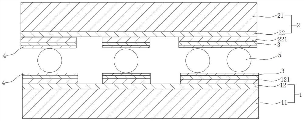
[0036] like figure 1 As shown, a liquid crystal antenna panel includes a first composite substrate 1 and a second composite substrate 2 oppositely arranged, and the first composite substrate 1 and the second composite substrate 1 are connected by a sealing frame between the first composite substrate 1 and the second composite substrate 2. The edge area between the two composite substrates 2 is closed to form a liquid crystal cavity filled with liquid crystal.

[0037] Please continue to refer to figure 1As shown, in some embodiments, the first composite substrate 1 includes a first flexible circuit board 12 and a first rigid substrate 11 for bonding and fixing with the first flexible circuit board 12; the second composite substrate 2 includes a second The flexible circuit board 22 and the second rigid substrate 21 are used to attach and fix the second flexible circuit board 22 . In some embodiments, the first flexible circuit board 12 includes a copper-clad flexible polyimid...

Embodiment 2

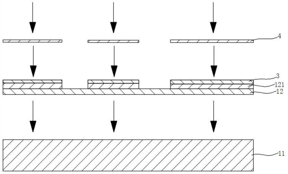
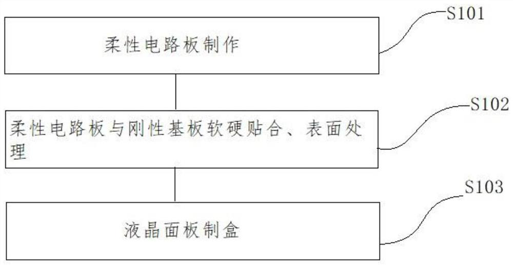
[0045] like image 3 As shown, the present application also relates to a manufacturing process of a liquid crystal antenna panel, comprising the steps of:

[0046] S101. Fabrication of flexible circuit boards;

[0047] S102, flexible circuit board and rigid substrate soft and hard lamination, surface treatment;

[0048] S103. Making boxes for liquid crystal panels.

[0049] Among them, S101, the production of flexible circuit boards includes:

[0050] Step 1. Cutting and cutting, cutting the copper-clad film of the large-area coil raw material, and cutting it to the required size. Here, the size of the flexible circuit board is between 50mm*50mm and 2000mm*2000mm;

[0051] Step 2, drilling, drilling the flexible circuit board, and drilling positioning holes, conduction holes, and test holes according to the circuit design. The positioning holes are used to facilitate subsequent processing and positioning. The first flexible circuit board and / or the first flexible circuit b...


PUM


Abstract

The invention relates to a liquid crystal antenna panel and a manufacturing process thereof, the liquid crystal antenna panel comprises a first composite substrate and a second composite substrate which are oppositely arranged, and a liquid crystal cavity filled with liquid crystal is formed between the first composite substrate and the second composite substrate; the first composite substrate comprises a first flexible circuit board and a first rigid substrate which is fixedly attached to the first flexible circuit board; and the second composite substrate comprises a second flexible circuit board and a second rigid substrate used for being fixedly attached to the second flexible circuit board. The problems that a traditional liquid crystal antenna panel is high in manufacturing cost, long in iteration production period and unstable in thick copper manufacturing process are solved, and the requirement for small-batch production or rapid research and development iteration is met.

Description

technical field [0001] The present application relates to the technical field of wireless communication, in particular to a liquid crystal antenna panel and a manufacturing process thereof. Background technique [0002] The liquid crystal antenna and its array phased array antenna based on liquid crystal (LC) material with good radio frequency performance are new products in the hot technical field of academia and engineering circles in recent years. Liquid crystal antenna is an important branch of electronically scanned (ESA) tunable phased array antenna, which can be widely used in millimeter wave and high frequency microwave antenna products. [0003] At present, the main technical solutions for liquid crystal antenna panels rely on traditional liquid crystal display panel production lines for production and manufacturing. However, the technology of the liquid crystal antenna panel needs to upgrade and transform the equipment of the traditional liquid crystal production ...

Claims


Application Information

Patent Timeline
Patent Type & Authority Applications(China)
IPC IPC(8): H05K3/00H05K1/02G02F1/1333
CPCH05K1/0283H05K3/0058G02F1/1333
Inventor 修威田海燕杨光李凯翔徐琦
Owner BEIJING HUAMETA TECH CO LTD
Why Eureka
Try Eureka