Defect detection method and system
A defect detection and to-be-detected technology, applied in optical testing flaws/defects, measuring devices, material analysis by optical means, etc., can solve problems such as circuit fabrication failures, reduce noise interference, and improve detection efficiency.
- Summary
- Abstract
- Description
- Claims
- Application Information
AI Technical Summary
Problems solved by technology
Method used
Image


Examples
Embodiment Construction
[0048] As mentioned in the background, there are still many problems in the defect detection process in the prior art. The following will describe in detail in conjunction with the accompanying drawings.
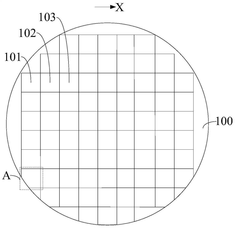
[0049] Figure 1 to Figure 4 It is a structural schematic diagram of each step of a defect detection method.
[0050] Please refer to figure 1 , providing a wafer 100 to be inspected, the wafer 100 to be inspected has a plurality of chips to be inspected, and the plurality of chips to be inspected include: a first adjacent chip to be inspected 101 arranged along a first direction X, a second The chip to be tested 102 and the third chip to be tested 103 .
[0051] Please refer to figure 2 , acquire the first image to be inspected 101a of the first chip to be inspected 101, the first image to be inspected 101a has several first pixel values to be inspected; obtain the second image to be inspected 102a of the second chip to be inspected 102, the said The second image to...
PUM
 Abstract
Description
Claims
Application Information
 - R&D
- Intellectual Property
- Life Sciences
- Materials
- Tech Scout
- Unparalleled Data Quality
- Higher Quality Content
- 60% Fewer Hallucinations
Browse by: Latest US Patents, China's latest patents, Technical Efficacy Thesaurus, Application Domain, Technology Topic, Popular Technical Reports.
© 2025 PatSnap. All rights reserved.Legal|Privacy policy|Modern Slavery Act Transparency Statement|Sitemap|About US| Contact US: help@patsnap.com